Isolated Power Supplies for Telecom Applications
To ensure compliance with all international standards, the designer of an isolated power supply for telecom applications needs to take certain facts into account: The input voltage is never 110V or 220V from the mains, but the lower voltage of a lead-acid battery (-12V, -24V, or -48V) that is charged by means of the mains through rectification (Figure 1). (Batteries back up the telecom system in case of failure in the mains supply.) To combat corrosion due to ion flow, the input voltage is always negative, with the positive terminal connected to ground.
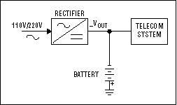
Figure 1. In this block diagram of the backup architecture used in telecom systems, a battery block is kept charged by the mains rectifier. In the event of a mains failure, it supplies the system to prevent transmission interruptions.
详情介绍
To ensure compliance with all international standards, the designer of an isolated power supply for telecom applications needs to take certain facts into account: The input voltage is never 110V or 220V from the mains, but the lower voltage of a lead-acid battery (-12V, -24V, or -48V) that is charged by means of the mains through rectification (Figure 1). (Batteries back up the telecom system in case of failure in the mains supply.) To combat corrosion due to ion flow, the input voltage is always negative, with the positive terminal connected to ground.
Figure 1. In this block diagram of the backup architecture used in telecom systems, a battery block is kept charged by the mains rectifier. In the event of a mains failure, it supplies the system to prevent transmission interruptions.
ISDN and other systems powered by a remote source often operate with a higher input voltage: up to 120VDC. (Losses due to line resistance are proportional to the square of supply current, so the lower supply current associated with higher input voltage allows a longer transmission line.) By powering the telecom phone through the cable as well as the local mains, such systems eliminate the need for a backup battery at the cable's user end. When required, the cable therefore carries both transmission signals and supply current (Figure 2).
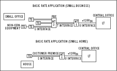
Figure 2. In an ISDN system for small-office or home applications, the phone lines normally carry forward transmissions. During emergencies, they carry power from the central office to the remote unit's network termination (NT) and terminal equipment (TE).
The selection of power-conversion topology depends on the level of output power required: forward or flyback for low power, push-pull for medium power, and half or full bridge for high power. The simplest configuration (flyback) stores energy in the transformer during the ON period of the primary PWM (when the power MOSFET is ON), and it releases it to the load during the OFF period (Figure 3). Because the secondary diode (D1) is forward-biased at that time, energy stored in the transformer goes to the load and charges the output capacitor. Energy stored in the output capacitor is delivered to the load during the next ON period. For this configuration, the primary-controller IC can have a fixed-frequency PWM configuration such as the MAX668 or a variable-frequency PFM configuration such as the MAX1771. A controller like the MAX5003 can be powered directly from the high input voltage.

Figure 3. A flyback converter stores energy during every cycle: in the transformer when the power MOSFET is ON and forward to the load when the power MOSFET is OFF.
In the forward topology (Figure 4), energy is forwarded to the secondary when the primary's power MOSFET turns ON. Energy is not stored in the transformer as in a flyback circuit, so the forward configuration allows a smaller transformer and more power output. An output inductor on the secondary side stores energy and also reduces ripple current in the output capacitor. During an ON period, the load receives energy directly from the transformer trough diode D1 and L1; however, during an OFF period, inductor L1 forces diode D2 to conduct. Thus, L1 and C1 together maintain a continuous delivery of energy to the load.
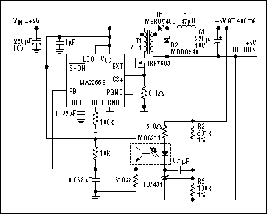
Figure 4. Because forward converters forward energy to the secondary side during every cycle, they don't require a large isolation transformer for storing energy.
The push-pull configuration (Figure 5) can be simplified as a double-forward converter in which the primary's two power MOSFETs alternate on and off. Energy-conversion principles for the push-pull and forward types are exactly the same during each half cycle, but push-pull circuits reset the transformer during each primary-to-secondary energy transfer (rather than during an OFF period). This action allows more output power for a given transformer geometry.
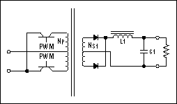
Figure 5. Push-pull converter.
Full-bridge configurations are generally used for power outputs over 1kW (Figure 6). They allow use of the transformer in two quadrants of the BH magnetization characteristic, rather than one as in the forward and flyback circuits (Figure 7). Also, the input-voltage swing seen by the transformer primary equals 2VIN rather than 1VIN. As the power MOSFET pair Q1/Q4 turns on together, then Q2/Q3, the transformer primary winding sees +VIN during the first cycle and -VIN during the second. Energy transfers to the load during each cycle of the secondary (as for the forward topology), but the better transformer optimization allows higher output power.
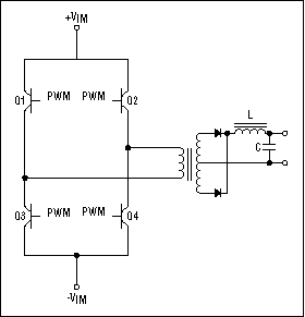
Figure 6. Full-bridge converter.
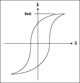
Figure 7. B-H magnetization shape of a magnetic material.
Yet other topologies are available. Resonant or quasi-resonant converters, for example (based on a resonant circuit inserted in the energy-conversion chain), reduce switching-power loss in the active element by avoiding square-wave signals of current and voltage. Whatever the topology, however, points common to all must be taken into consideration:
- EMI/RFI
- Safety
- Transient-voltage protection
- Output overcurrent and overvoltage protection
- Operating temperature and thermal protection
- Feedback
EMI/RFI
High-frequency operation (to 1MHz and higher) of the transformers in today's switching power supplies allows a reduction in all dimensions of those magnetic components. On the other hand, the high-frequency square waves (PWM or PFM topologies) or sine waves (resonant or quasi-resonant topologies) produce electromagnetic emissions during every cycle of energy transfer. International standards define limits for these emissions, which are conducted by the input and the output cables as EMI and radiated from space around the power supply as RFI.
The international specification for conducted EMI and radiated RFI is EN55022, which lists maximum allowable amplitudes for EMI in the range 150kHz to 30MHz (Table 1) and for RFI in the range 30MHz to 1000MHz (Table 2). EN55022 also defines the tests needed for verifying compliance with its requirements, and it delineates the conditions necessary for approval of the laboratory in which the tests are conducted. Products that fail to meet these specifications for electromagnetic compatibility cannot be branded with the CE mark for sale in the European community or with UL approval for sale in the United States.
To meet specified limits for EMI and RFI, you must consider certain points during the design. First, identify sources of noise and minimize them as much as possible. In the 100kHz flyback topology in Figure 3, for example, five noise sources are easily identified:
1. Rise and fall time at the power MOSFET T1: According to Fourier analysis, this square wave can be regarded as a sum of harmonics: the first at 100kHz, the second at 200kHz, the third at 300kHz, etc., all with progressively lower amplitudes. Reducing the switching waveform's dV/dT minimizes the high-frequency harmonics, but a limit is imposed by the power dissipated during turn-on and turn-off.
2. T1 turn-off: During T1's turn-off, parasitic inductance and capacitance in the circuit and the transformer cause higher-frequency ringing in the drain voltage. This ringing energy can be minimized by specifying a transformer with small leakage inductance and by adding a diode/resistor/capacitor snubber circuit.
3. Ringing in D1: Similarly, an undesired noise frequency (ringing) due to parasitic capacitance in the secondary diode D1 can be reduced by a resistor/capacitor network in parallel with the diode.
4. RFI from the transformer: RFI noise caused by the flyback transformer's air gap can be reduced several decibels by shielding the transformer with copper foil.
5. Layout: All components carrying the switching waveform should be as small as possible, with short connections. A long connection can act as an antenna, transmitting unwanted noise almost everywhere.
In 99% of all cases, you can reduce the problem (but not solve it completely) by taking all these principles into account. They entail the cost of extra parts. Noise coming from the power supply and present at the battery input, for example, must be attenuated with an EMI filter that consists of a differential inductor, a common-mode inductor, and ceramic or high-frequency capacitors. It is impossible, however, to define a standard series of EMI filters that accommodates all different circuit topologies and output-power levels.
A number of the elements involved in noise generation are not predictable by analysis. Only when the power supply has been implemented physically can you perform the analysis and experimental tests that enable design of the EMI filter. To allow a reasonable spread of component values during production, this filter should have approximately 10dB margins on the specification limits.
Introducing a capacitor between primary and secondary provides a low-impedance path for high frequencies. This capacitor (usually a ceramic type with a value of 1nF to 4.7nF or so) forces noise to flow through the converter internally, thereby lowering the noise on both sides of the power supply by several decibels. Radiated noise is generally suppressed by placing the complete converter with an EMI filter in a six-sided metallic box.
Safety
For secondary outputs to be defined as telecom extra-low voltage (TELV), they must be isolated from the input side of the converter. TELV outputs can be touched by an operator without any particular attention or protection. For this purpose, the international specifications EN60950 and UL950 define minimum isolation voltages between input and output, and minimum-allowed distances between primary and secondary parts of the converters. Refer to Tables 3 and 4 (in EN60950).
As shown in these tables, the minimum-allowed creepage and clearance distances¹ depend on the construction technology, the working environment, and the operating voltage. As an example, for an input voltage of 76VDC, a pollution degree² of 3, and reinforced insulation, the creepage and clearance distances are 2mm and 4mm, respectively.
You can easily implement a safety area on the printed circuit board in which the only component between primary and secondary sections is the power transformer. This transformer must incorporate the safety distances required by international specifications (enameled copper cannot be defined as insulation).
Four main technologies are available for meeting the safety-insulation requirements in transformer construction, each with its own advantages and disadvantages. Each of these approaches is examined below, with respect to a four-winding transformer in which the primary winding is split in two parts: _-Primary/Secondary/Auxiliary-secondary/_-Primary.
1. One approach provides insulation by sleeving the beginning and the end of each winding (Figure 8). Windings are placed 2mm from the border of the coil former. Total creepage distance between two windings is 2mm+2mm = 4mm. (Only 2mm are necessary, but the additional 2mm margin can improve yields and manufacturing time during production.) Because enameled copper is not considered insulation, the ends of each winding must be protected by an insulating material; otherwise, the creepage distance is reduced to less than 2mm.
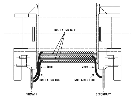
Figure 8. The insulation in this cross section of a wound transformer consists of sleeving and insulating tape. Because sleeves are defined as insulation, this approach lets you reduce the safety distances by a factor of two.
Additional insulating material is required between the primary and the secondary windings. If reinforced or double insulation is needed, there must be at least two layers of insulation. Because it allows good coupling between windings, this production technology minimizes leakage inductance and is useful in constructing transformers with multiple secondary outputs. It also allows a good compromise on delivered watts per unit volume of transformer. Because protection sleeves cannot be placed automatically, the manual work required makes this technique quite expensive.
2. Another method entails providing insulation by placing the primary windings close to one side of the coil former and the secondary windings on the other side (Figure 9). Distance is kept at 4mm, but coupling between windings is very poor. This approach is almost impossible for small transformers.
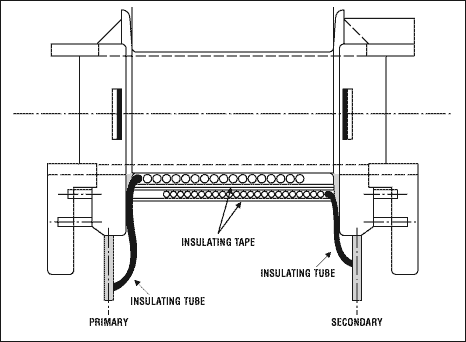
Figure 9. This is a cross section of a wound transformer, in which the insulation is provided by insulating tape (enameled copper is not defined as insulation). Safety regulations mandate the minimum distances between windings.
3. The use of special wire for the secondary winding, covered by two layers of insulating material (recognized by UL as double insulation), can be a solution for small-geometry transformers. This approach can be automated up to 100%. On the other hand, the high cost of the wire required makes it less attractive.
4. A coil former consisting of two concentric half sections in which all the primaries are contained in one section and all the secondary windings in the other allows efficient assembly of the transformer. The two concentric parts are first wound separately (primary windings in one, secondary windings in the other) and then joined in a second operation. This process can be automated completely. It reduces manual re-work almost to zero and yields the least expensive transformer of its type available today. Coupling between primary and secondary is poor, however, and (unfortunately) the split-primary transformer under examination cannot be built this way. This approach is of great interest for low-power transformers in flyback topologies that operate from the 120VAC mains (a cellular-phone battery charger, for example).
Minimizing mechanical dimensions is a common requirement for telecom converters in PC-board applications. Because safety specifications define a minimal creepage distance related to the pollution degree of the external environment, you can improve the pollution degree and reduce creepage distance by placing the transformer in a box filled with resin, under vacuum. By modifying the transformer's internal environment this way, a pollution degree of 1 is easily achievable (refer to Table 4).
Transient-Voltage Protection
Virtually all electrical equipment is subject to excessive voltage pulses during normal operation. Such pulses can be generated by lightning or by nearby electrical equipment such as large electrical motors. International specifications EN61000-4-5 and EN41003 define the pulse types that certified equipment must be able to withstand.
In telecom power supplies operating from rectified voltage, a 1.5kW transient-voltage suppressor (TVS) is generally sufficient to protect the supply and meet all the international specifications necessary for CE approval. More complex is the protection of an RS232 or RS485 interface used for maintenance and communications inside the end equipment. It can be expensive to place a TVS on each line, especially if the lines must maintain low parasitic capacitance to support high transmission data rates.
A wide choice of RS-232 and RS-485 interface ICs for this purpose are available from Maxim. All include ESD protection tested per IEC1000 specifications at levels up to ±15kV. That spec ensures an interface compliant with the CE requirements, without need for further tests in production.
Output Overcurrent and Overvoltage Protection
Output protection prevents damage to the power supply as a consequence of load currents ranging from zero to that of a short-circuited output, as well as damage to the load as a result of irregular supply voltage caused by such faults. The following is an examination of two circuits: one to protect the power supply from unusual load currents and the other to protect the load from unusual output voltages.
Telecom power supplies require a constant output-current characteristic. When load current exceeds a certain level, generally 20% to 40% above the nominal value (Inom), the converter output becomes a constant-current generator. For that condition, reducing load resistance only lowers the output voltage.
In terms of power management, the worst-case condition for such telecom supplies is the worst-case maximum load current (Inom plus 40%), which occurs when the output voltage is still regulated. Delivered power is 40% above nominal and can persist indefinitely. The entire power supply must be capable of withstanding this level of output power. Because the necessary over specification can affect mechanical dimensions and price of the heatsink, a system can benefit by restricting the allowed tolerance on output current. Maxim offers a wide choice of high-side precision current monitors for this purpose, ranging from the simple MAX4173 in a SOT23 package (Figure 10) to the MAX471, which can also detect the current flow direction.
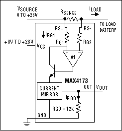
Figure 10. In high-side current measurements, the MAX4173 provides a voltage referred to ground and proportional to current flowing in the sense resistor.
These ICs employ a resistor in series with the load current that drops only a few millivolts, thanks to an internal current mirror that produces, in a resistor referenced to ground, an analog voltage proportional to the high-side load current. For the MAX471, this measurement has an accuracy of ±2%. A simple op amp such as the MAX4040 can act on this signal to generate current-protection feedback that acts directly in the converter's voltage feedback loop. It affects the feedback loop only when output-current protection is invoked. Although power-supply stability for that condition must also account for the current-protection circuit's response time, stability is seldom compromised because the required response time is not fast.
Multiple outputs (main plus auxiliary voltages) can be protected by devices such as the MAX869L and the MAX890L. In addition to current-measurement circuitry, these ICs include a power MOSFET in series with the measured load current, which can disconnect the load in response to overcurrent conditions. All these current measurements are performed on the positive rail, i.e., on the output. The alternative (measuring on the negative rail, or the common of the power supply) includes all current returned by the system. For a three-output system, for example, this means that every output must be designed to withstand all the current. Such negative-path loops in a complex system can actually produce wrong current measurements.
Because any failure within the converter can cause an out-of-spec output voltage with a catastrophic effect on the load, most systems include a simple circuit that monitors the output voltage continuously and stops the converter in case of an over- or undervoltage condition. Maxim offers a wide choice of such voltage monitors, such as the MAX6806. When the monitor reports a voltage failure via a protection loop, it must first stop the primary IC controller. If the failure persists, it must also (through a driver circuit) turn on an SCR connected in parallel with the converter's output. Once the SCR turns on, it can exit from the ON latching condition only when its current flow falls to zero.
Not all load circuits like to endure the dv/dt of a converter output as it rises from zero to nominal during turn-on. Most prefer to remain in a reset condition until the output voltage stabilizes. Maxim is the worldwide leader in generating such resets during startup. Simple ICs like the MAX809 or the MAX6351, for example, available in SOT23 packages and able to monitor 1 or more voltages, provide a "Power OK" signal with delay (typically 140mS). They also advise the system, with considerable precision, to save all necessary data before a declining supply voltage disappears completely.
Operating Temperature, Flammability, and Thermal Protection
UL 94VO, V1 or V2, defines limits for the maximum temperature inside an electrical system. Tests performed by qualified personnel in a certified laboratory must verify compliance before a UL stamp on the system can be approved. Thus, the thermal-management aspect of power-supply design should ensure, for the sake of system reliability, that the temperature of any hot spot caused by worst-case conditions remain within specified limits.
The more critical components in a power converter are generally the primary power switches, the secondary rectifier diodes, and the isolating transformer. Good thermal coupling between the active components and a heatsink is desirable, unless the increased parasitic capacitance between the switch element and the heatsink exacerbates EMI.
High-temperature wire and insulating material per UL specifications ensures a high operating temperature for the isolation transformer. All materials must have a self-extinguish rating per UL94V0, 94V1; the use of such materials simplifies final UL recognition for the system. Even if the thermal operating temperature of a telecom system is defined by specification, an over- or undertemperature condition during normal operation (mainly over-) can have a catastrophic effect on the power supply. Barring immediate failure, the temperature fault can reduce equipment life by lowering the MTBF of components stressed by the hot temperature.
To avoid irreversible damage, thermal protection should include a double threshold: a logic alarm to advise that temperature is going out of specification and a second alarm (with a higher threshold) that shuts down the converter. Thermal protection must be placed close to the most critical component; that component is identified easily in a thermal map produced with an infrared camera.
Maxim's MAX6501/6502 thermal sensors monitor the ambient temperature with high accuracy and provide a logic signal when the threshold is reached. When compared with the traditional thermal switch, their high precision, semiconductor reliability, small mechanical dimensions (SOT23 packages), and low prices make them very attractive. MAX6503/6504 sensors for negative temperatures can advise when the temperature is lower than a specified minimum value; this is a condition that can affect the converter's ability to start up. An undertemperature logic signal can turn on a heat generator.
Feedback
The regulated output of a telecom power supply is generally tight (±5%), but in some cases greater accuracy is required. Influences that must be opposed in maintaining tight output accuracy include the effects of load variation (load regulation), line-voltage variation (line regulation), and temperature. Thus, the controller on the primary side must receive feedback from the regulated output voltage on the secondary side. To maintain the inherent isolation between primary and secondary windings, this feedback signal should be isolated as well. Three circuits are useful for this function:
- Feedback via auxiliary transformer windings
- Feedback via optocouplers
- Feedback via extra magnetic parts, which allow communication between the primary and the secondary circuits
Feedback based on an auxiliary transformer winding is very simple. The auxiliary-winding voltage, which usually supplies the primary side of the converter, is monitored by the primary controller. Coupling between secondary and auxiliary windings cannot be very tight, because safety demands creepage and clearance, and double or more insulation between them. As a result, the typical tolerance on an auxiliary-winding voltage is only 10%. Some loads can tolerate this loose tolerance; others employ post-regulation in the form of a synchronous step-down converter such as the MAX1623 or the MAX1714. Major advantages for the auxiliary-winding approach include small size and a low-cost control circuit.
To obtain optocoupler feedback, an op amp on the secondary side (such as the MAX4122) continuously compares the output voltage with that generated by a voltage reference (such as the MAX6002). The op-amp output then drives the optocoupler diode, producing a feedback signal from the optocoupler proportional to the error difference between output and reference voltages. That is, a current transfer between the diode and the transistor (isolated from each other) produces a current output on the primary side. Flowing through a resistor, this current produces the signal voltage read by the primary-side controller (Figure 3).
By offering a wide choice of optocouplers already approved for this function by the safety agency, today's market aids safety qualification of the power supply. To further simplify procurement, all components in this circuit are standard parts.
For feedback using extra magnetic parts (which allow communication between the primary and the secondary circuits), the principle is the same as for an optocoupler. The secondary circuit is somewhat complex in this case, because the magnetic parts must be driven by a signal of a certain frequency rather than a DC current. The resulting extra expense of the feedback element (magnetic part) makes this solution less interesting, except for particular applications such as space equipment, in which the higher reliability of a magnetic part is appreciated.
Closing a feedback loop means designing a high-gain wide-bandwidth circuit that allows a fast response to line and load variations. Limits imposed by stability considerations, however, usually compel a compromise on the response time. Two parameters must be defined: crossover frequency (fC) and phase margin.
Overall gain in the feedback path (op amp, optocoupler, and primary controller) has a certain bandwidth, and the corner is that frequency at which the gain equals 1 (0dB). The op amp's inverting configuration introduces a 180° phase shift in the signal (negative feedback), and additional phase lag is introduced by the compensation network. Thus, the signal can exhibit a phase shift of 180° plus 180° or more, producing positive feedback that results in oscillation of the output voltage.
According to Nyquist, a system is stable if the added phase shift at fC is less than 180°. Therefore, a key parameter in power-supply design is phase margin at fC, defined as follows: How many degrees must be added to the feedback phase shift to obtain 180°?
Practical experience with various topologies has shown that a phase margin of 45° allows good load regulation with acceptable overshoot and undershoot, without permitting fast transients to trigger oscillation. Another good compromise is to limit the corner frequency: fC < fSWITCHING/(2x3.14xD), where D is the maximum duty cycle.
Every power-supply feedback loop must be designed. Bode plots, offering a simple picture of gain and phase for the different elements, give an overall result when you add the pictures together (Figure 11). Bode says the gain slope for a single pole above its corner frequency is -20dB/decade and its phase shift is 90°. Thus, a double-pole LC network has a gain slope of -40dB/ decade above its corner frequency and a phase shift of 180°.
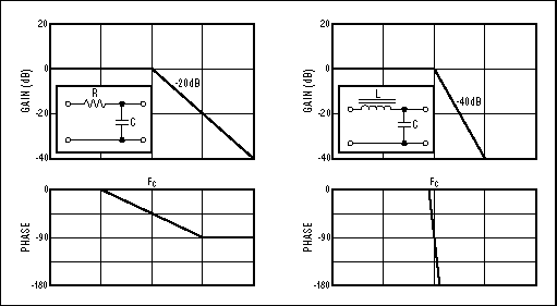
Figure 11. These Bode plots depict a single-pole RC network and a double-pole LC network.
As an example, consider the compensation of a power supply operating at 70kHz with a duty cycle of 50%, described by the power-supply characteristic of Figure 12. The maximum corner frequency is fSWITCHING/(2x3.14xD) = 22kHz. Beyond this corner frequency, the output capacitor, the inductor, and the load resistor produce a -40dB/decade attenuation and a 180° phase shift. The op amp's bandwidth is more than 10MHz, but its associated RC components introduce a pole and zero, to compensate phase lag introduced by the LC pole and to provide at least 45° of phase margin at fC.
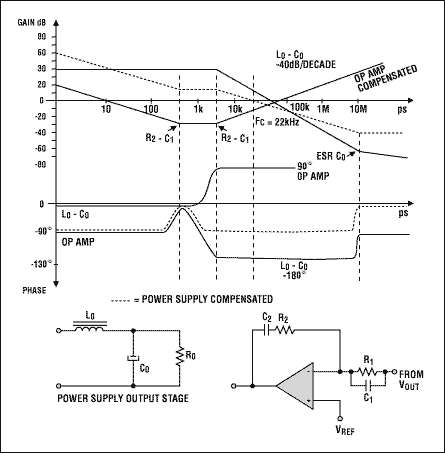
Figure 12. Simplified Bode plots depict a power-supply output and its compensation network.
To ensure good output-voltage regulation at DC, a pole in the error amplifier reduces the gain by -20dB/decade. A zero caused by R2-C2 modifies the gain slope to 0dB/decade, and R2-C1 causes a gain increase to +20dB/decade. As a result, phase introduced by the compensated op amp starts at -90° (due to the first pole), goes to 0° (due to R2-C2), and rises to +90° (due to R2-C1). Summing the output-LC and compensated-op-amp characteristics gives the overall result (dotted line), which indicates a power supply compensated with fC = 22kHz and a phase margin of 90°.
________________________
¹Per the American UL Standard (also adopted by the European EN60950 Standard), clearance is the minimum-allowed distance specified for separation of uninsulated conductive surfaces of opposite polarity. Creepage is a corresponding distance between two such surfaces, measured along any connecting surfaces (rather than the line-of-sight through-air distance specified for clearance).
²Per the American UL Standard (also adopted by the European EN60950 Standard), pollution degree 2 environments can have nonconductive contaminants or temporary conductivity caused by condensation. Pollution degree 3 environments can have conductive contaminants.