LFRD001: MAX1472/MAX1473/MAXQ610 Remote Keyless Entry Reference Design
General Description
The MAX1472 transmitter and MAX1473 receiver reference design (RD) is a self-contained evaluation platform for exercising both products as a remote keyless entry (RKE) demonstrator system. With the use of the MAXQ® USB-to-JTAG board (MAXQJTAG-USB), the MAXQ610 microcontroller on both the transmitter key fob board and the receiver board can be programmed by the end user.
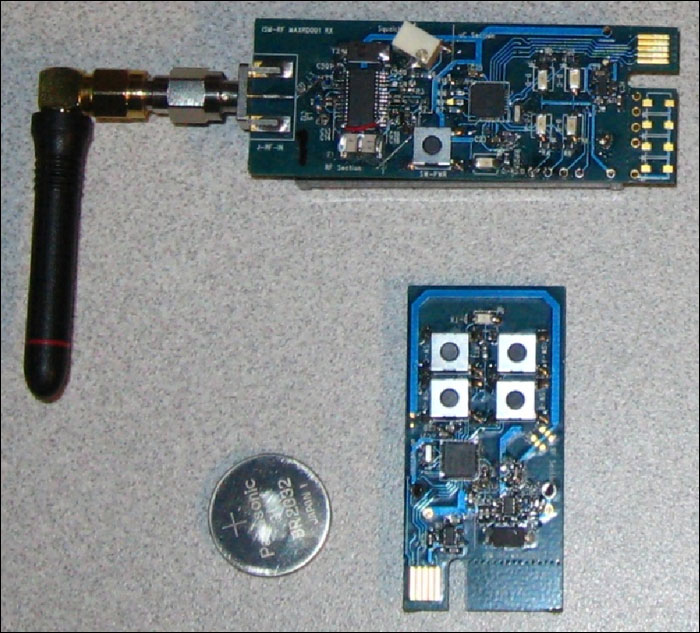
A simple interface is provided on the transmitter (Tx) board, including four independent momentary switches and a user feedback LED. The Tx board includes a built-in printed-circuit board (PCB) antenna and operates off of a single CR2032 coin cell battery. The receiver (Rx) board includes one momentary switch and five LED connections to the microcontroller. An SMA connector is provided for attaching various Rx antennas, allowing the user to test different designs. The receiver is powered from a pair of AAA batteries.
Both the Tx and Rx boards are usable as-is. Gerber files are available for simple cut-and-paste designs of either the radio sections or the full implementation.
Features
- Proven PCB layout
- Proven component parts list
- Preprogrammed Tx/Rx pair for quick demonstration capabilities
- Free MAXQ microcontroller programming tools available for flexible operation
Quick Start
- Pull the two boards (Tx and Rx) out of box and install the CR2032 and two AAA batteries.
- Connect the Rx antenna.
- Press and hold the SW-PWR button on the Rx board for approximately 4 seconds and release the button after the LEDs blink.
- Press any button on the Tx (this will "pair" the two boards).
- Press any button on the Tx to see the matching LED light up on the Rx.

详情介绍

Click here for an overview of the wireless components used in a typical radio transceiver.
General Description
The MAX1472 transmitter and MAX1473 receiver reference design (RD) is a self-contained evaluation platform for exercising both products as a remote keyless entry (RKE) demonstrator system. With the use of the MAXQ® USB-to-JTAG board (MAXQJTAG-USB), the MAXQ610 microcontroller on both the transmitter key fob board and the receiver board can be programmed by the end user.
A simple interface is provided on the transmitter (Tx) board, including four independent momentary switches and a user feedback LED. The Tx board includes a built-in printed-circuit board (PCB) antenna and operates off of a single CR2032 coin cell battery. The receiver (Rx) board includes one momentary switch and five LED connections to the microcontroller. An SMA connector is provided for attaching various Rx antennas, allowing the user to test different designs. The receiver is powered from a pair of AAA batteries.
Both the Tx and Rx boards are usable as-is. Gerber files are available for simple cut-and-paste designs of either the radio sections or the full implementation.
Features
- Proven PCB layout
- Proven component parts list
- Preprogrammed Tx/Rx pair for quick demonstration capabilities
- Free MAXQ microcontroller programming tools available for flexible operation
Quick Start
- Pull the two boards (Tx and Rx) out of box and install the CR2032 and two AAA batteries.
- Connect the Rx antenna.
- Press and hold the SW-PWR button on the Rx board for approximately 4 seconds and release the button after the LEDs blink.
- Press any button on the Tx (this will "pair" the two boards).
- Press any button on the Tx to see the matching LED light up on the Rx.
Transmitter and Receiver Board Description
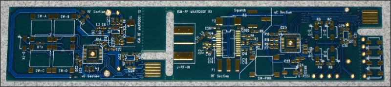
Unpopulated Rev B boards.
Form Factor
The LFRD001 was designed as a demonstration platform for the MAX1472 transmitter and the MAX1473 receiver. This reference design targets a low-cost, low-BOM-count RF link. Both the transmitter and the receiver are mated with a MAXQ610 microcontroller that is preprogrammed to operate as an RKE demonstration system.
Both boards were designed to allow the end user to program the MAXQ610 through a JTAG interface. To make the demonstrator even more flexible, the JTAG edge-connectors can be snapped off of both boards, accommodating an even smaller profile. In its smallest form, the Tx board is 1in. x 1.75in. (2.54cm x 4.45cm) and the Rx board is 1in. x 2.4in (2.54cm x 6.1cm). The Rx board can be configured to display the LEDs, either flush with the PCB itself (as installed) or with the included break-away section. With the latter option, the user can vertically mount (or remote cable mount) the LEDs for better viewing.
Populated Rev B boards.
I/Os and Switches
Power is typically supplied to the Tx board by a CR2032 battery, but can alternatively be powered through the JTAG interface. The Rx board is powered by a pair of AAA batteries and also has the JTAG power provision.
| Tx Switch Function Table | |||
| Switch | Position | Function | µC Connection |
|---|---|---|---|
| SWA | Momentary | "Red" channel | Pin 9, P1.0 |
| SWB | Momentary | "Green" channel | Pin 10, P1.1 |
| SWC | Momentary | "Blue" channel | Pin 11, P1.2 |
| SWD | Momentary | "White" channel | Pin 12, P1.3 |
| Rx Switch Function Table | |||
| Switch | Position | Function | µC Connection |
|---|---|---|---|
| SW-PWR | Momentary | Tx pairing | Pin 10, P1.1 |
| Tx and Rx I/O Edge Connectors | ||
| Signal | Description | µC Connection |
|---|---|---|
| JTAG-1 | TCK—clock | Pin 24, P2.4 |
| JTAG-2 | GND—ground | |
| JTAG-3 | TDO—data out | Pin 27, P2.7 |
| JTAG-4 | VBAT—external supply | |
| JTAG-5 | TMS—master select | Pin 26, P2.6 |
| JTAG-6 | nRST—reset | Pin 28, Reset |
| JTAG-7 | N/A | |
| JTAG-8 | N/A | |
| JTAG-9 | TDI—data in | Pin 25, P2.5 |
| JTAG-10 | GND—ground | |
| Tx LED Indicator Table | ||
| LED | Function | µC Connection |
|---|---|---|
| D-TX | Reset/active transmission | Pin 21, P1.7 |
| Rx LED Indicator Table | ||
| LED | Function | µC Connection |
|---|---|---|
| D-A | "Red" channel indicator | Pin 16, P1.4 |
| D-B | "Green" channel indicator | Pin 17, P1.5 |
| D-C | "Blue" channel indicator | Pin 20, P1.6 |
| D-D | "White" channel indicator | Pin 21, P1.7 |
| D-RSI | Receive signal indicator | Pin 12, P1.3 |
Data Frame Structure
The basic structure of the data frame is amplitude-shift keying (ASK) modulated, Manchester encoded, and 4.8kbps (0.2083ms/bit). It also has 144 bits per frame (18 bytes or nine 2-byte words), 30ms per frame, a pause of 70ms between frames, and 3 frame transmissions per burst. For information on Manchester encoding, refer to application note 3435, "Manchester Data Encoding for Radio Communications."
| Frame Structure | |||||||||||||||||
| Preamble | ID | Function | Data | Sync | Bat | Sig | Chk Sum | ||||||||||
|---|---|---|---|---|---|---|---|---|---|---|---|---|---|---|---|---|---|
| FF | FF | FF | FD | 01 | 23 | 45 | 67 | 00 | 01 | 00 | 00 | 43 | 21 | 11 | 22 | 01 | 68 |
The structure of this frame is arbitrary but provides an example of the information that can be contained in any frame related to the many industrial, scientific, medical (ISM) RF applications. Appendix I describes each section of the data frame in more detail.
Firmware Structure
Transmitter
Functional operation of the Tx system is much more basic than that of the Rx system. The MAXQ610 microcontroller provides two inputs to the MAX1472: ENABLE and DATA. The transmission is controlled by a simple button press on one of the four buttons: SW-A, SW-B, SW-C, or SW-D. The MAXQ610 is configured to be in a stop mode unless it senses a high-to-low transition on one of the four buttons, causing an external interrupt. The interrupt is serviced by first decoding which switch has been closed, assigning a function code to the frame corresponding to that switch, and then completing a Manchester-encoded broadcast of the packetized bits. The transmitter is enabled and each Manchester half-bit is sent serially to the DATA line with appropriate timing. After the frame is complete, the transmitter is turned off for a set amount of time until it either repeats the frame transmission or the MAXQ610 is released back to "stop mode" (no further button presses). See Appendix II for the Tx firmware code.
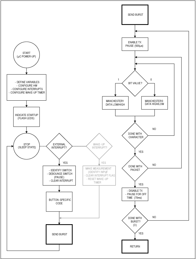
Figure 1. Tx subroutines.
Receiver
The receiver is a complex system requiring data filtering, timing recovery, frame alignment, Manchester decoding, checksum evaluation, and a display function. The MAXQ610 microcontroller is configured with two external interrupts: one from the SW-PWR button and the other from the MAX1473 DATAOUT line. When an interrupt is received, the microcontroller will evaluate whether to flag the pairing process or to decode incoming data. A transmission will be received as an expected bit stream of Manchester-encoded 4.8kbps data. After performing a lowpass filter (LPF) type of noise reduction, the data is stored in an array and then processed for valid structure. The checksum is verified and if the ID matches the one stored in the receiver (if from the paired Tx), the frame "function" is acted upon. See Appendix II for the Rx firmware code.
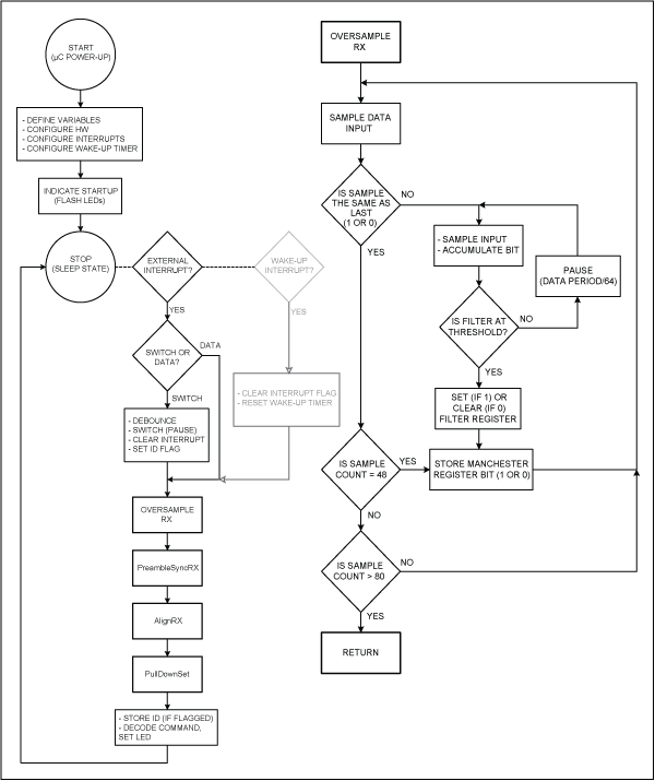
Figure 2. Rx subroutines.
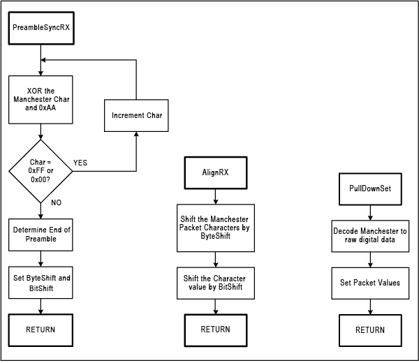
Figure 3. Rx subroutines.
Microcontroller Programming Software
The above firmware was developed within the IAR Embedded Workbench® software. A full version of this software (4k KickStart Edition) can be obtained online with a limited license that restricts the object code to 4k in size. Commercial licenses can also be purchased from IAR. The IAR EW works in concert with the MAXQUSB-JTAG interface and the programming adapter, to flash the MAXQ610 on both the Tx and Rx boards.
Installation
Refer to the IAR EW documentation for installation and guidance. The firmware in this project was developed with the MAXQ plug-in IAR EWMAXQ2.20I.
Operation
Be sure to have the USB port properly configured within the IAR EW: Project ![]() Options...
Options... ![]() General Options—Debugger—JTAG. The COM Port should be set to match the "USB Serial Port (COM XX)" as indicated in the Windows® Device Manager.
General Options—Debugger—JTAG. The COM Port should be set to match the "USB Serial Port (COM XX)" as indicated in the Windows® Device Manager.
For best performance during programming and debugging of the MAXQ610, we suggest adjusting the advanced settings for the COM port (Device Manager ![]() USB Serial Port (COM XX) Properties
USB Serial Port (COM XX) Properties ![]() Port Settings
Port Settings ![]() Advanced...). Recommended values for receive and transmit buffer sizes are 512 bytes and a recommended latency timer of 4ms provides optimal operation.
Advanced...). Recommended values for receive and transmit buffer sizes are 512 bytes and a recommended latency timer of 4ms provides optimal operation.
The edge connector should be oriented with JTAG pin 1 on the top of the Tx or Rx boards. The system can be programmed with batteries in place or without any batteries installed (USB power is used). Within the C code, there are some lines that can be uncommented to help debug firmware changes.
Operational Setup and Use
Pairing the Tx and Rx
In this reference design, the transmitter has been preprogrammed with a semi-unique ID (0x012345XX). This 4-byte value has been flashed into the MAXQ610 as part of the firmware-encoding process and can be easily changed by reprogramming the Tx microcontroller. To link the receiver system to the transmitter system, the user simply needs to set the "pair" flag on the receiver and send a valid signal with the transmitter to be paired. This process must be repeated whenever the batteries are replaced on the Rx system.
- Press and hold the button (SW-PWR) on the Rx system for approximately 4 seconds.
- Once the Rx system cycles through the four LEDs (two repetitions), release the button.
- Press any button on the Tx system to be paired.
- The Rx system will again cycle all four LEDs (two repetitions) when a valid frame is received.
- The Tx and Rx systems are now paired. Test the link with any button press on the Tx.
Range
The predicted range in a flat unobstructed outdoor area is based on the following assumptions.
f0 = 433.92MHz
PPA = +10dBm
GT = -18dBi (small loop antenna typical -18dBi)
hTX = 1m
hRX = 1m
GR = 4.14dBi (ideal 1/4λ antenna = 5.14dBi)
LConR1 = -0.57dB
Path loss varies as R-4 because of ground bounce interference
RX sensitivity set at -114dBm
The calculated estimate of "open field" range is approximately 230m (see application note 5142, "Radio Link-Budget Calculations for ISM-RF Products" for more information).
Indoor range testing resulted in a consistent range of 30m using a Linx RX antenna; 35m was achieved with a 1/4λ antenna on the Rx with it placed ~2m above the floor; 30m was also reached in a lab environment with the Rx 1m above the floor. Outdoor testing resulted in a > 50m range. The LEDs could not be seen beyond 50m, and the actual range is likely greater.
Battery Usage Analysis
Microcontroller
[1.8V nominal core voltage, 1.0V RAM (min) data retention/power-on-reset (POR) voltage]
The MAXQ610 microcontroller burns a maximum of 12µA (with power-fail off) during stop mode.
The MAXQ610 (with 12MHz SysClk) burns a maximum of 5.1mA during normal operation.
Tx
The MAX1472 transmitter burns a maximum of 1.73µA at 125°C in standby mode.
The MAX1472 typically burns 9.6mA at 434MHz (~17mA max) during normal operation with "always on"; it typically burns 5.7mA when running at 50% duty cycle at 434MHz.
The LED is configured with 75Ω limiting resistors, yellow (VF = 2.2), nominal 10.7mA on current.
The Panasonic CR2032 battery has a rated 225mAh capacity.
With the LED off, the typical full-on battery life is about 15 hours. With the Tx duty cycle of 50% (Manchester), and for 30ms transmissions with 70ms "quiet time" between repeated bursts, the microcontroller is on full time [30ms at 5.7mA, 70ms at 1.8µA + 5.1mA], and the battery life jumps to about 33hrs. Given a 3-second button press, this would equate to about 39.6k button presses from a single battery. At an estimated 10 presses a day, this equates to about 10.8 years of battery life (worst-case scenario without LED usage).
During testing, measured current draws were ~69µA during standby mode and ~16mA peak current during transmission (including LED, 3.0V supply). These values would result in approximately 0.37 years of battery life for standby mode only. This system has not yet been optimized for low-current stop mode.
Rx
The MAX1473 receiver burns a maximum of 5.3µA at 434MHz during power down or sleep mode.
The MAX1473 burns a maximum of 6.88mA at 434MHz during normal operation.
The LEDs are all configured with 75Ω limiting resistors: red (VF = 2.0), nominal 13.3mA on current; green (VF = 2.1), nominal 12.0mA on current; blue (VF = 3.5), tested 3.5mA (at 3.0V supply) on current; white (VF = 3.5), tested 2.1mA (at 3.0V supply) on current; yellow (VF = 2.2), nominal 10.7mA on current.
The AAA batteries have a typical capacity of about 1000mAh at a drain current of 12mA (1.0V, 20°C).
When all of the LEDs are off, the typical complete battery life is about 3.47 days. With a Rx duty cycle of about 2ms on, 198ms off (1%), the battery life jumps to 1511 days (198ms at 18µA, 2ms at 12mA = 27.564µA). Thus, with the system always on, the Rx board will operate for about 4.1 years from a pair of AAA batteries (worst-case scenario without LED usage).
During testing, the measured current drain was ~9.5mA during listen mode and about 22mA peak current during receive (including LEDs, 3.0V supply). These values result in approximately 4.4 days of battery life for listen mode only. This system has not yet been optimized for mid-low current standby mode or low-current stop mode.
Hardware Details
Transmitter Specifications
| Supply current (IDD) at fRF = 433MHz, Tx "0" | 1.7mA (typ) |
| Supply current (IDD) at fRF = 433MHz, Tx "1" | 9.6mA (typ) |
| Standby current (ISTDBY) | 1.7µA (max) |
| Low-power standby current (ENABLE "0") | 5nA (typ) |
| Output power (POUT) into 50Ω at VDD = 2.7V | +10.3dBm (typ) |
Receiver Specifications
| Supply current (IDD) at fRF = 433MHz, 3.3V | 5.8mA (typ) |
| Shutdown supply current (I%-overbar_pre%PWDN%-overbar_post%) at fRF = 433MHz, 3.3V | 5.3µA (max) |
| Sensitivity (PRFIN_MIN) (peak power level) | -114dBm (typ) |
Ordering Information
| Part | Temp Range |
|---|---|
| MAX-ISMRF-RD001 | 0°C to 70°C |
Component List
The following table provides a list of components used to populate the Tx, Rx, and programming adapter boards. Maxim recommends high-quality, wire-wound inductors for components used on both the Tx and Rx boards.
| Designation | Qty | Description |
|---|---|---|
| 1 | Edge connector | |
| 1 | MAXQUSBJTAG-KIT# | |
| 1 | 433MHz antenna | |
| 1 | CR2032 battery | |
| 2 | AAA battery | |
| BATT-2032 | 1 | BATT-2032, BATT-2032 |
| BATT-AAA | 1 | BATT-2AAA, 2 AAA battery |
| C2, C26 | 3 | CAP, 0.01µF, 10% |
| C21–22, C24–25 | 4 | CAP, 0.1µF, 10% |
| C3, C17 | 2 | CAP, 0.47µF, 10% |
| C20, C23 | 2 | CAP, 1.0µF, 10% |
| C8, C11, C13–14 | 4 | CAP, 100pF, 5% |
| C16 | 1 | CAP, 1500pF, 5% |
| C18 | 1 | CAP, 150pF, 5% |
| C12 | 1 | CAP, 2.2pF, 5% |
| C27–28 | 2 | CAP, 2.2µF, 10% |
| C1, C6, C15 | 3 | CAP, 220pF, 10% |
| C19 | 1 | CAP, 330pF, 10% |
| C4–5, C500–501 | 4 | CAP, 6.8pF, 5% |
| C7 | 1 | CAP, 680pF, 10% |
| C9 | 1 | CAP, 7.5pF, 5% |
| Y3–4 | 2 | CERAMIC-SMD, 12.000MHz |
| F1 | 1 | FLT\MURATA\SFTLA10M7FA00-B0, 10.7MHz |
| L5 | 2 | IND-MOLDED, 24nH, 5% |
| L2 | 1 | IND-MOLDED, 51nH, 5% |
| L3 | 1 | IND-MOLDED, 56nH, 5% |
| L1 | 1 | IND-MOLDED, 62nH, 5% |
| D-RSI, D-TX | 2 | LED-1 (yellow) |
| D-A | 1 | LED-1 (red) |
| D-B | 1 | LED-1 (green) |
| D-C | 1 | LED-1 (blue) |
| D-D | 1 | LED-1 (orange) |
| U1 | 1 | MAX1472AKA+ |
| U2 | 1 | MAX1473EUI+ |
| U6 | 1 | MAX8887EZK33 |
| U3–4 | 2 | MAXQ610A-0000+ |
| R1, R3, L4 | 3 | RES, 0Ω |
| R7, R14 | 2 | RES, 100Ω |
| R6 | 1 | RES, 200kΩ |
| R2 | 1 | RES, 5.6kΩ |
| RA, RB, RC, RD, RRSI, RTX | 6 | RES, 75Ω, 1% |
| J-RF-IN | 1 | SMA |
| SW-A, SW-B, SW-C, SW-D, SW-PWR | 5 | SW-SPST-NO-B, SPST NO |
| Y2 | 1 | XTAL-SMD, 13.2256MHz |
| Y1 | 1 | XTAL-SMD, 13.560MHz |
| 1 | PCB (Tx and Rx boards) |
Schematics
(Revision C1: a detailed copy is available here.)
Tx Blocks
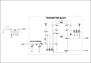
More detailed image (PDF, 253kB)
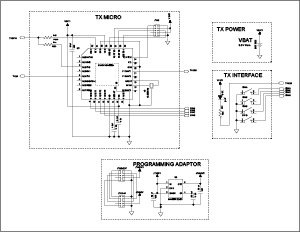
More detailed image (PDF, 270kB)
RX Blocks
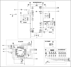
More detailed image (PDF, 470kB)
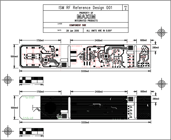
Layout
(Revision C1: detailed scale plots are available here.)
Related Application Notes
Application note 1954, "Designing Output-Matching Networks for the MAX1472 ASK Transmitter"
Application note 2815, "Calculating the Sensitivity of an ASK Receiver"
Application note 3401, "Matching Maxim’s 300MHz to 450MHz Transmitters to Small Loop Antennas"
Application note 3435, "Manchester Data Encoding for Radio Communications"
Application note 3671, "Data Slicing Techniques for UHF ASK Receivers"
Application note 4302, "Small Antennas for 300MHz to 450MHz Transmitters"
Application note 4314, "Getting Started with the MAXQ610 Evaluation Kit (EV Kit) and the IAR Embedded Workbench"
Application note 4465, "Using the Serial Port on the MAXQ610 Microcontroller"
Application note 4636, "Avoid PC-Layout "Gotchas" in ISM-RF Products"
Application note 5142, "Radio Link-Budget Calculations for ISM-RF Products"
Appendix I: RKE Frame Structure
The basic structure of the data frame is ASK modulated, Manchester encoded, 4.8kbps (0.2083ms/bit). It also has 144 bits per frame (18 bytes or nine 2-byte words), 30ms per frame, pause of 70ms between frames, and 3 frame transmissions per burst. For information on Manchester encoding, refer to application note 3435, "Manchester Data Encoding for Radio Communications."
| Frame Structure | |||||||||||||||||
| Preamble | ID | Function | Data | Sync | Bat | Sig | Chk Sum | ||||||||||
|---|---|---|---|---|---|---|---|---|---|---|---|---|---|---|---|---|---|
| FF | FF | FF | FD | 01 | 23 | 45 | 67 | 00 | 01 | 00 | 00 | 43 | 21 | 11 | 22 | 01 | 68 |
The structure of this frame is arbitrary but has been established to provide an example of the information that can be contained in any frame related to the many ISM-RF applications.
| Preamble | |||
| Preamble | |||
|---|---|---|---|
| FF | FF | FF | FD |
The default preamble for this reference design is 4 bytes of high data with a pair of stop bits at the end. Since this is transmitted with Manchester encoding, the waveform appears as a 4.8kHz square wave lasting for 6.67ms. Having a preamble longer than roughly 1ms should provide ample time for the Rx system to wake up, given a strong received signal strength. The MAX1473 has a typical wake-up time of 250µs to start receiving valid data. Extra time can be padded onto this initial wake-up time to allow the Rx system to properly settle the baseband slicing circuit, which in turn provides optimum sensitivity. Providing a preamble of over 6ms gives ample opportunity for a relatively weak signal to wake up the receiver.
Assuming the MAXQ610 microcontroller used in the Rx is sitting in a stop mode, the system will consume a certain number of received bits to start up the microcontroller before it can begin decoding the data stream. The nanopower ring oscillator in the MAXQ610 typically runs at 8kHz (the wake-up timer interval can be 1/fNANO to 65535/fNANO). If the Rx system is configured to use the RXSIG or the RXDATA line as an interrupt generator, the µC would have a warm-up time of 8192 × tHFXIN. With tHFXIN = 83.3ns (fXCLK= 12MHz clock), the warm-up time works out to approximately 0.6827µs. This is well within the time available in one preamble transmission, and at a baud rate of 4.8kbps, the µC should be in a warmed-up state within 3.28 bits. The FD pattern at the end of the preamble is used to indicate the following start of the data frame and is the key to synchronizing the received bit stream.
| ID Structure | |||
| ID | |||
|---|---|---|---|
| 01 | 23 | 45 | 67 |
The ID section is configured with 4 bytes of identification. This permits 232 unique identifiers or over 4.29 billion codes. If one byte is used for class identification (256 different car models for example), 224 unique identifiers or over 16 million codes remain. The structure can be modified to suit the purpose of the user. This RD has been preprogrammed to use an identification code as noted above, with the last byte being adjusted between RD systems. This allows for simultaneous operation of multiple, independent RKE systems.
| Function Structure | |
| Function | |
|---|---|
| 00 | 01 |
This simple reference design has only four input switches on the transmitter, so 2 bytes of "function" is overkill. Again, this structure can be modified to suit the purposes of the user. In this application, when button A is pressed, the function value is 00 01. When button B is pressed, the function value is 00 02, and so forth. The function value is used to convey information (with individual buttons having their own bit), so it is possible to indicate multiple button presses simultaneously. In this instance, if buttons B and D were pressed together, the function value would be represented as 00 0A (this multibutton operation has not been implemented in the design). This is an arbitrary definition for the structure of the function value and it can always be modified by the user.
| Data Structure | |
| Data | |
|---|---|
| 00 | 00 |
The data section of this frame is provided for transmitting information such as a temperature or pressure measurement, a speed indicator, etc. In this design, the data section could work in concert with the function section to convey information whenever a button on the transmitter has been pressed. Again, the use of this data value is arbitrary and can be modified by the user. This operation is not currently implemented in the design.
| Sync Structure | |
| Sync | |
|---|---|
| 43 | 21 |
The synchronization block is set up to provide for encryption coding. Users can work with this section to provide rolling code sync, a public key, etc. This operation is not currently implemented in the design.
| Battery Gauge Indicator |
| Bat |
|---|
| 11 |
This single byte allows the transmitter to send an indication of battery strength to the receiver. This section of the frame could have value when indicating a need to change the Tx battery. This operation is not currently implemented in the design.
| Signal Strength Indicator |
| Sig |
|---|
| 22 |
A possible use for a transceiver configuration, the received signal strength of the return channel could be shared between the nodes. This operation is not currently implemented in the design.
| Checksum | |
| Chk Sum | |
|---|---|
| 01 | 67 |
In this reference design, the checksum is used as a go/no-go gate for valid data. The frame values (except the preamble) are summed up during transmission, one byte at a time, and the full sum is tacked on to the end of the frame as the checksum. This value is compared to a received data stream and a decision to use or discard the frame is made. The format of this checksum operation is arbitrary, but as long as the Tx, Rx, and encode/decode methods are equivalent, the checksum process will operate as intended.
Appendix II: Tx Firmware
main.h (17 Jun 2010, Rev 0.3):
/****************************************************************************
* Copyright (C) 1999-2012 Maxim Integrated, All Rights Reserved.
*
* See main.c for additional information.
*
******************************************************************************/
/* Main Subroutines */
void Lights3();
void ExtISR();
void SwitchPress();
void BuildPacket();
void SendBurst();
void WUSample();
void Pause(long int Count);
/* ------------------------------------------------------------------------- */
/* Global Constants */
static int IntFlag = 0;
static int PacketChars = 18;
static char Preamble[4] = {0xFF,0xFF,0xFF,0xFD},
ID[4] = {0x01,0x23,0x45,0x67},
Func[2] = {0x00,0x00},
Data[2] = {0x00,0x00},
Sync[2]= {0x43,0x21},
Bat = 0x11,
Sig = 0x22,
CheckSum[2] = {0x00,0x00};
static char Packet[19]; // store the packet data as a string: 18 char + null
static int BitMask[8] = {128, 64, 32, 16, 8, 4, 2, 1}; // store a bit mask
static int SleepTime = 0x0FA00; // ~ 8sec sleep time (almost max)
static int TXWUCnt = 273; // TX Warm-Up Count (~500us)
static int ManCnt = 61; // pause time for 1/2 Manchester bit
static long int TXOffCnt = 40000; // TX Off time Count
/* ------------------------------------------------------------------------- */
See the latest LFRD001-RXcode.zip file for all the Rx firmware code.
main.c
isr.c
iomacro.h
iomaxq.h
iomaxq61x.h
iomaxq610.h
RD001-RX.dep
RD001-RX.ewd
RD001-RX.ewp
RD001-RX.eww
Appendix III: RX Firmware
main.h (17 Jun 10, Rev 0.3):
/****************************************************************************
* Copyright (C) 1999-2012 Maxim Integrated, All Rights Reserved.
*
* See main.c for additional information
*
******************************************************************************/
/* Main Subroutines */
void Lights6();
void SwitchInt();
void ExtISR();
void OversampleRX();
void PreambleSyncRX();
void AlignRX();
void PullDownSet();
char PullDownPair(short int MPIndex);
int Validate();
int Paired();
void WURX();
void Pause(long int Count);
/* ------------------------------------------------------------------------- */
/* Global Constants / Variables */
static int IntFlag = 0;
static char ManPacket[39]; // store the Manchester data of with 2x18+1 char
// packet (including full preamble) + 2 'noise' characters
static int ByteShift = 0;
static int BitShift = 0;
static char ID[4] = {0x00,0x00,0x00,0x00}, // storage of the RX data
Func[2] = {0x00,0x00},
Data[2] = {0x00,0x00},
Sync[2]= {0x00,0x00},
Bat = 0x00,
Sig = 0x00,
CheckSum[2] = {0x00,0x00};
static char PairID[4] = {0x00,0x00,0x00,0x00}; // initial paired ID
static int PairON = 0; // flag to indicate the pairing function
/* ------------------------------------------------------------------------- */
See the latest LFRD001-TXcode.zip file for all the Tx firmware code.
main.c
isr.c
iomacro.h
iomaxq.h
iomaxq61x.h
iomaxq610.h
RD001-TX.dep
RD001-TX.ewd
RD001-TX.ewp
RD001-TX.eww
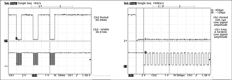
Appendix IV: Tx and Rx Timing
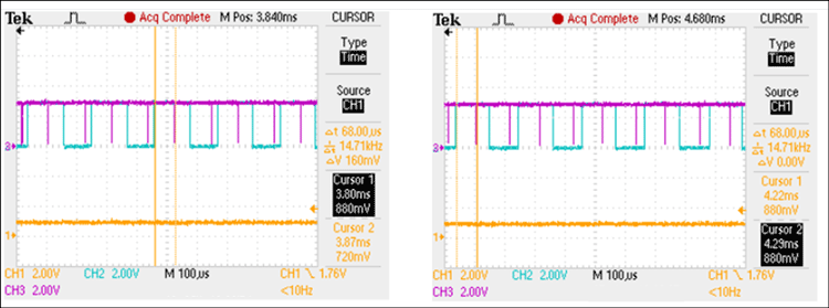
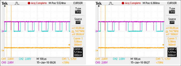
The plots below show the three packet transmissions (with appropriate "dead time" between packets) and the individual bit timing of the transmitted data. The top trace is the ENABLE line to the transmitter and the bottom trace is the DATA line, both generated by the MAXQ610.
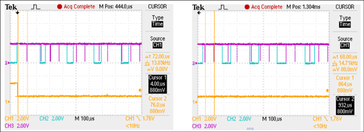
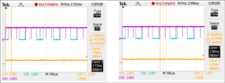
The following series of oscilloscope captures represent the first portion of an incoming transmission packet. The orange trace is the RSI signal, which is generated by the MAXQ610 as soon as an external interrupt is processed. The blue trace is the DATAOUT signal generated by the MAX1473 and the magenta trace is a debug signal (see the OversampleRX routine in the Rx code) indicating when the MAXQ610 stores the DATAOUT logic value. The initial Manchester-encoded packet values can be seen as FF FF FF FD. Note there is a duty cycle skew to the DATAOUT signal caused by the MAX1473 baseband data slicer circuit tracking to a midlevel. This skew causes a number of missampled data values, which are ignored by the PreambleSyncRX routine.
IAR Embedded Workbench is a registered trademark of IAR Systems AB.
MAXQ is a registered trademark of Maxim Integrated Products, Inc.
Windows is a registered trademark and registered service mark of Microsoft Corporation.
Windows XP is a registered trademark and registered service mark of Microsoft Corporation.