OCEANSIDE (MAXREFDES9#):3.3V至15V输入、±15V (±12V)输出、隔离电源

详情介绍
Introduction
| The Oceanside design (MAXREFDES9#) uses a step-up controller (MAX668), a 36V H-bridge transformer driver (MAX13256), and a pair of low dropout (LDO) linear regulators (MAX1659 x2) to create a ±15V (±12V) output isolated power supply from a wide range of input voltages. This general purpose power solution can be used in many different types of isolated power applications, but is mainly targeted for industrial sensors, industrial automation, process control, and medical applications. | 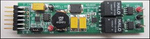 More detailed image (PDF, 1.8MB) |
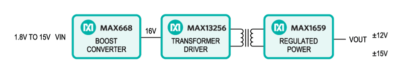
Figure 1. The Oceanside subsystem design block diagram.
Features |
Applications |
|
|
Detailed Description of Hardware
The Oceanside subsystem reference design operates from a 3.3V to 15V DC power source. The MAX668 high-efficiency step-up controller boosts the input voltage to 16V and connects to the input of the H-bridge transformer driver. The MAX13256 H-bridge transformer driver switches at 425kHz and drives the primary side of the 1:1 turns ratio, with the use of TGMR-501V6LF transformers from Halo® Electronics. The full-wave bridge rectifiers convert the AC outputs of the Halo transformers’ secondary coils into DC outputs. The LDOs regulate the voltages to ±15V. The Zener diodes (D3 and D4) protect the LDOs by keeping their input voltages below 16.5V.
The output current of the H-bridge transformer driver is limited to 300mA by the R5 2.2kΩ resistor, which protects the LDO from overcurrent. The following equation sets the current limit for the H-bridge transformer driver.
R5 (kΩ) = 650/ILIM (mA)
Having a step-up controller before the H-bridge transformer driver gives users the advantage of not needing to change the transformers to get a different turns ratio when a different input supply voltage is applied.
The input power is selectable by JU1. Place the shunt on the 1-2 position to power the board by an external power supply connected to the VIN and GND1 connectors. Place the shunt on the 2-3 position to power the board by the J1 Pmod-compatible connector.
To change the output voltage of this subsystem reference design, simply change the feedback resistors (R7–R10) of the LDOs (U3 and U4), and also change the feedback resistors (R3 and R4) of the step-up controller (U1).
The output voltage of the MAX668 step-up controller is set by the following equation:
VOUT = VSET × (1 + R7/R9) for U3
VOUT = VSET × (1 + R8/R10) for U4 Where
VSET = 1.21V The output voltage of the MAX668 step-up controller is set by the following equation:
VOUT = VSET × (1 + R3/R4) Where VSET = 1.25
For example, for the ±12V output application, change R7 and R8 to 90.9kΩ, and change R9 and R10 to 10.2kΩ. The output of the LDOs becomes ±12V when their inputs (outputs of the transformers and the full-wave bridge rectifiers) are higher than 12V plus the dropout voltage. Next, change R3 to 100kΩ and R4 to 10.5kΩ to set the output of the step-up controller to 13.15V (slightly higher than 12V plus the dropout voltage and two diode voltage drops from the full-wave bridge rectifier). It is important to not set this voltage too much higher than the output of LDOs, because the extra power would be lost in the LDOs and thus efficiency would be lower. In applications that are sensitive to output voltage ripple, a lowpass LC pi filter can be added in front of the LDO input.
The isolation transformer in this design has an isolation voltage of 5000VRMS. It is recognized by UL 60950 and EN 60950 and falls into the "functional" insulation class.
Quick Start
Required equipment:
- Oceanside (MAXREFDES9#) board
- 3.3V to 15V power supply
- Two digital voltmeters
Procedure
The Oceanside board is fully assembled and tested. Follow the steps below to verify board operation.
- Place the shunt on jumper JU1 to the 1-2 position.
- Connect the positive terminal of the power supply to the VIN connector.
- Connect the negative terminal of the power supply to the GND1 connector.
- Connect the positive terminal of the first voltmeter to the +15V connector.
- Connect the negative terminal of the first voltmeter to the GND2 connector.
- Connect the positive terminal of the second voltmeter to the -15V connector.
- Connect the negative terminal of the second voltmeter to the GND2 connector.
- Turn on the power supply.
- Use the respective voltmeters to measure the corresponding positive and negative output voltages.
Lab Measurements
The Oceanside design was tested with two pairs of output voltage rails: ±15V and ±12V. Other voltage rails can be achieved by modifying the resistor value ratios of R3/R4, R7/R9, and R8/R10. Equal loads on both rails were used when testing the Oceanside design. Table 1 shows the maximum load for various setups. The maximum load is recorded when the output voltage drops to 1% less than the designed output voltage. The power efficiency (as shown in Figures 2 to 8) is calculated with the sum of the output power on both rails divided by the input power.
For asymmetrical load applications, the maximum load can be larger for one rail and less for the other rail. To achieve a larger maximum load, the user can increase the output voltage of the step-up controller, but the efficiency will decrease due to the higher voltage drop across the LDO.
Table 1. Maximum Load for Test Setups
| Input Voltage (V) | Output Rail (V) | Maximum Load (Equal Loads Applied to Both Rails) (mA) | Efficiency at Maximum Load (%) |
|---|---|---|---|
| 3.3 | ±15 | 65 | 78 |
| 5 | ±15 | 70 | 79 |
| 12 | ±15 | 85 | 83 |
| 15 | ±15 | 90 | 86 |
| 3.3 | ±12 | 75 | 77 |
| 5 | ±12 | 80 | 78 |
| 12 | ±12 | 100 | 83 |
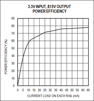 Figure 2. Power efficiency vs. current load for a 3.3V input to a ±15V output. |
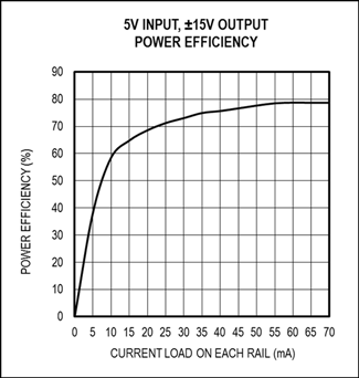 Figure 3. Power efficiency vs. current load for a 5V input to a ±15V output. |
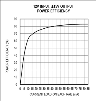 Figure 4. Power efficiency vs. current load for a 12V input to a ±15V output. |
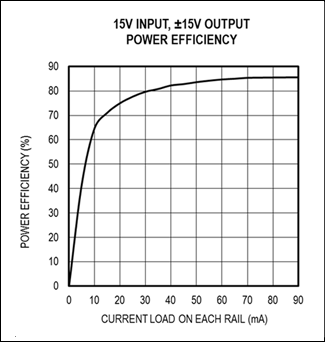 Figure 5. Power efficiency vs. current load for a 15V input to a ±15V output. |
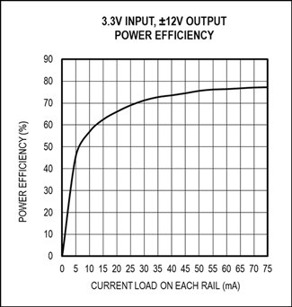 Figure 6. Power efficiency vs. current load for a 3.3V input to a ±12V output. |
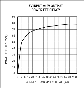 Figure 7. Power efficiency vs. current load for a 5V input to a ±12V output. |
 Figure 8. Power efficiency vs. current load for a 12V input to ±12V output. |
|
The output noise is well below 0.5% of the output voltages. The noise is mainly caused by the switching pulses of the MAX13256. Figures 9 to 16 show the scope shots of the noise for various setups. The noises on the negative rails are identical to those on the positive rails for symmetrical load applications.
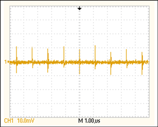 Figure 9. Noise for VIN = 3.3V, VOUT = 15V, IOUT = 0mA. |
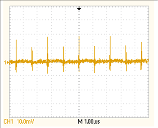 Figure 10. Noise for VIN = 3.3V, VOUT = 15V, IOUT = 65mA = maximum load. |
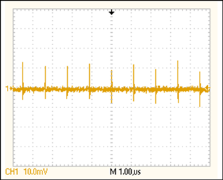 Figure 11. Noise for VIN = 15V, VOUT = 15V, IOUT = 0mA. |
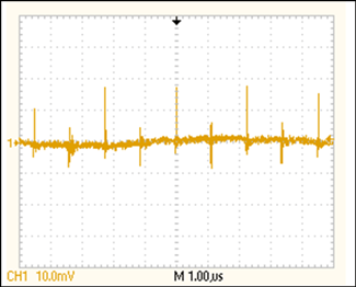 Figure 12. Noise for VIN = 15V, VOUT = 15V, IOUT = 90mA = maximum load. |
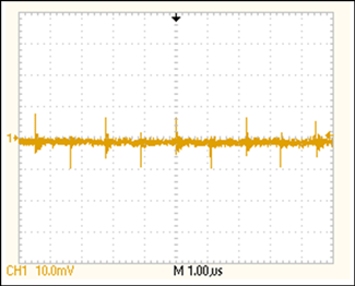 Figure 13. Noise for VIN = 3.3V, VOUT = 12V, IOUT = 0mA. |
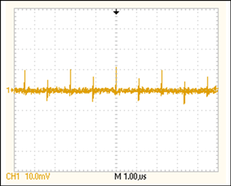 Figure 14. Noise for VIN = 3.3V, VOUT = 12V, IOUT = 75mA = maximum load. |
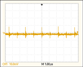 Figure 15. Noise for VIN = 12V, VOUT = 12V, IOUT = 0mA. |
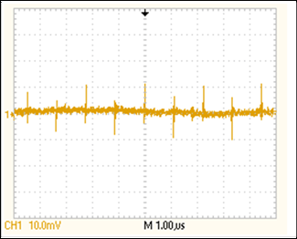 Figure 16. Noise for VIN = 12V, VOUT = 12V, IOUT = 100mA = maximum load. |