SANTA FE (MAXREFDES5#):16位、高精度、多路输入、隔离型模拟前端(AFE)


概述
当今内置模/数转换器(ADC)的现场可编程门阵列(FPGA)和微控制器支持低分辨率和低电压模拟输入。然而,这些ADC不能满足要求较高分辨率和较高输入电压的工业控制和工业自动化应用的需求。Santa Fe (MAXREFDES5#)子系统设计为16位、高精度工业模拟前端(AFE),支持-10V至+10V、0至10V和4–20mA电流环路信号,具有隔离电源和数据通路,集成在小尺寸外形封装中。Santa Fe设计集成低噪声、高阻模拟缓冲器(MAX9632);带有创新片上衰减的高精度ADC(MAX1301);超高精度4.096V电压基准(MAX6126);600VRMS数据隔离(MAX14850);隔离/稳压+12V、-12V和5V 电源(MAX256/MAX1659)。该AFE方案可用于需要高精度模/数转换的任何应用,但主要目标应用为工业传感器、工业自动化、过程控制、可编程逻辑控制器(PLC)和医疗应用。
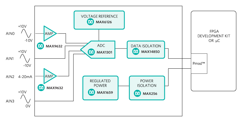
图1. Santa Fe子系统设计方框图。
特性 |
应用 |
|
|
详情介绍
Introduction
Today's field programmable gate arrays (FPGAs) and microcontrollers with internal analog-to-digital converters (ADCs) are capable of low-resolution and low-voltage analog inputs. However, they fall short on being able to meet the needs of industrial control and industrial automation applications, where isolation, higher resolutions, and higher voltage system solutions are often needed. The Santa Fe (MAXREFDES5#) subsystem reference design is a 16-bit high-accuracy industrial analog front end (AFE) that accepts -10V to +10V, 0 to 10V, and 4–20mA current loop signals with isolated power and data integrated into a small form factor. The Santa Fe design integrates low-noise high-impedance analog buffers (MAX9632); a highly accurate ADC with innovative on-chip attenuation (MAX1301); an ultra-high precision 4.096V voltage reference (MAX6126); 600VRMS data isolation (MAX14850); and isolated/regulated +12V, -12V, and 5V power rails (MAX256/MAX1659). This AFE solution can be used in any application that needs high-accuracy analog-to-digital conversion, but it is mainly targeted for industrial sensors, industrial automation, process control, programmable logic controllers (PLCs), and medical applications.
Figure 1. The Santa Fe subsystem design block diagram.
| Features | Applications |
|---|---|
|
|
Detailed Description of Hardware
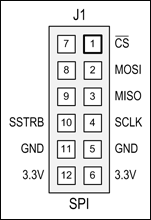
The Pmod specification allows for both 3.3V and 5V modules as well as various pin assignments. This module is designed only for a supply voltage of 3.3V and uses the SPI pin assignments as illustrated on the right.
The power requirements are shown in Table 1. The currently supported platforms and ports are shown in Table 2.
Table 1. Power Options for the Santa Fe Subsystem Reference Design
| Power Type | Jumper Shunt | Input Voltage (V) | Input Current (mA, typ) |
|---|---|---|---|
| On-board isolated power | JU3: 1-2 JU4: 2-3 JU5: 1-2 |
3.3 | 221 |
| External power | JU3: 2-3 JU4: 1-2 JU5: 2-3 |
3.3 | 6.3 |
| +12 | 30.4 | ||
| -12 | 7.3 |
Table 2. Supported Platforms and Ports
| Supported Platforms | Port |
|---|---|
| Nexys™ 3 Platform (Spartan®-6) | JB1 |
| ZedBoard™ platform (Zynq®-7020) | JA1 |
| MicroZed™ platform (Zynq-7010) | J5 |
The Santa Fe hardware design is specifically optimized for applications that use -10V to +10V, 0 to 10V, and 4–20mA signals. Depending on the application requirements, certain portions of the circuit may be omitted. A complete discussion of what portions are needed or may be omitted follows. See the file for the schematic under the All Design Files section.
The MAX1301 (U3) is a 16-bit, successive-approximation register (SAR) ADC with unique multirange inputs capable of accepting input voltage signals up to +12.288V to -12.288V. The ADC also has integrated analog input buffers with a 17kΩ input resistance.
The first MAX9632 amplifier (U1) is optimized for low-noise, -10V to +10V input voltages. The second MAX9632 amplifier (U2) is optimized for low-noise, 4–20mA input currents. Both U1 and U2 provide high input impedance for input signals that have a large source resistance, or in the case of the 4–20mA loop, a 250Ω load resistance. Large source resistances often attenuate signals by an undesirable factor. Add an optional 500Ω series resistor in front of both MAX9632 amplifiers if input protection is desired while the Santa Fe design is not powered. The 500Ω series resistor prevents the input current from exceeding the maximum input current specification when 10V is applied at the input and the Santa Fe board has no power.
If the signal source has a significantly low source resistance compared to 17kΩ, or in the case of the 4–20mA loop, if the parallel combination of 250Ω and 17kΩ provides acceptable accuracy in the application, then U1 and U2 can be eliminated. ADC channels AIN1 and AIN3 are examples of using only the internal 17kΩ analog input buffers.
Although the MAX1301 ADC has an internal 4.096V voltage reference, for highest accuracy use the external MAX6126 (U4) voltage reference with 0.02% initial accuracy and a 3ppm/°C maximum temperature coefficient (tempco).
The MAX256 (U5) provides an isolated, functional insulation class power solution that accepts 3.3V and converts it to ±12V using an off-the-shelf TGM-H281NF Halo® transformer with a 1:2.6 primary to secondary turns ratio plus an external on-board voltage-doubler circuit. Post-regulation is accomplished using the MAX1659 low dropout (LDO) regulators. The ±12V isolated power solution is optional and is only needed for applications that require the MAX9632 amplifiers to provide a high input impedance or when power isolation is required. If the MAX9632 amplifiers are not needed, then a single +6V isolated supply can power the entire circuit. Data isolation is also optional depending on the application and is accomplished using the MAX14850 (U9) digital data isolator. The combined power and data isolation achieved is 600VRMS.
Detailed Description of Firmware for Nexys 3 Platform
The Santa Fe firmware design was initially released for the Nexys 3 development kit and targeted a MicroBlaze™ soft core microcontroller placed inside a Xilinx® Spartan-6 FPGA. Support for additional platforms may be added periodically under Firmware Files in the All Design Files section. The currently supported platforms and ports are shown in Table 2.
The firmware is a working example of how to interface to the hardware, collect samples, and save them to memory. The simple process flow is shown in Figure 2a. The firmware is written in C using the Xilinx SDK tool, which is based on the Eclipse™ open source standard. Custom Santa Fe-specific design functions were created utilizing the standard Xilinx XSpi core version 3.03a. The SPI clock frequency is set to 3.125MHz.
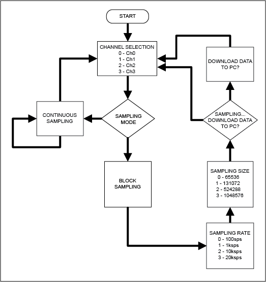
Figure 2a. The Santa Fe firmware flowchart for Nexys 3 platform.
The firmware accepts commands, writes status, and is capable of downloading blocks of sampled data to a standard terminal program via a virtual COM port. The complete source code is provided to speed up customer development. Code documentation can be found in the corresponding firmware platform files.
Detailed Description of Firmware for ZedBoard Platform
The Santa Fe firmware design supports the ZedBoard kit and targets a hardcore ARM® Cortex®-A9 processor inside the Xilinx Zynq system-on-chip (SoC).
The firmware is a working example of how to interface to the hardware, collect samples, and save them to memory. The simple process flow is shown in Figure 2b. The firmware is written in C using the Xilinx SDK tool, which is based on the Eclipse open source standard. Custom Santa Fe-specific design functions were created utilizing the ARM’s internal SPI peripheral instead of the standard AXI Xilinx XSpi core to increase the maximum sampling rate to 90ksps. The SPI clock frequency is set to 3.57MHz.
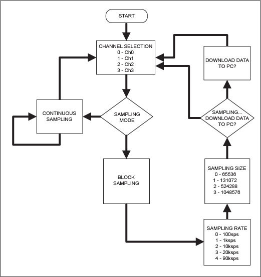
Figure 2b. The Santa Fe firmware flowchart for ZedBoard platform.
The firmware accepts commands, writes status, and is capable of downloading blocks of sampled data to a standard terminal program via a virtual COM port. The complete source code is provided to speed up customer development. Code documentation can be found in the corresponding firmware platform files.
Quick Start
Required equipment:
- Windows® PC with two USB ports
- Santa Fe (MAXREFDES5#) board
- Santa Fe-supported platform (i.e., Nexys 3 development kit or ZedBoard kit)
- Industrial sensor or signal source
Download, read, and carefully follow each step in the appropriate Santa Fe Quick Start Guide:
Santa Fe (MAXREFDES5#) Nexys 3 Quick Start Guide.
Santa Fe (MAXREFDES5#) ZedBoard Quick Start Guide.
Lab Measurements
Equipment used:
- Audio Precision® SYS-2722 signal source or equivalent
- Windows PC with two USB ports
- Santa Fe (MAXREFDES5#) board
- Nexys 3 development kit
- +12V power supply (for external power testing only)
- -12V power supply (for external power testing only)
Special care must be taken and the proper equipment must be used when testing the Santa Fe design. The key to testing any high-accuracy design is to use sources and measurement equipment that are of higher accuracy than the design under test. A low distortion signal source is absolutely required in order to duplicate the results presented below. The input signal was generated using the Audio Precision SYS-2722. The analog inputs should be driven with a source and not be left floating. The FFTs were created using the FFT control in SignalLab from Mitov Software. Table 3 provides a quick reference for the AC and DC performance of each channel for both on-board isolated power and external power shown in Figures 3 through 18. All lab measurements were done at room temperature.
Table 3. Quick Reference Guide for AC Performance (FFTs) or DC Performance (Histograms) in Figures 3 through 18
| Channel | Power Type | Input Type | Test Type | Figure Number |
|---|---|---|---|---|
| Channel 0 (AIN0) | On-board isolated | ±10V, High | AC - FFT | Figure 3 |
| Channel 0 (AIN0) | On-board isolated | ±10V, High | DC - histogram | Figure 4 |
| Channel 0 (AIN0) | External | ±10V, High | AC - FFT | Figure 5 |
| Channel 0 (AIN0) | External | ±10V, High | DC - histogram | Figure 6 |
| Channel 1 (AIN1) | On-board isolated | ±10V, 17kΩ | AC - FFT | Figure 7 |
| Channel 1 (AIN1) | On-board isolated | ±10V, 17kΩ | DC - histogram | Figure 8 |
| Channel 1 (AIN1) | External | ±10V, 17kΩ | AC - FFT | Figure 9 |
| Channel 1 (AIN1) | External | ±10V, 17kΩ | DC - histogram | Figure 10 |
| Channel 2 (AIN2) | On-board isolated | 4–20mA, 250Ω | AC - FFT | Figure 11 |
| Channel 2 (AIN2) | On-board Isolated | 4–20mA, 250Ω | DC - histogram | Figure 12 |
| Channel 2 (AIN2) | External | 4–20mA, 250Ω | AC - FFT | Figure 13 |
| Channel 2 (AIN2) | External | 4–20mA, 250Ω | DC - histogram | Figure 14 |
| Channel 3 (AIN3) | On-board isolated | 0 to 10V, 17kΩ | AC - FFT | Figure 15 |
| Channel 3 (AIN3) | On-board isolated | 0 to 10V, 17kΩ | DC - histogram | Figure 16 |
| Channel 3 (AIN3) | External | 0 to 10V, 17kΩ | AC - FFT | Figure 17 |
| Channel 3 (AIN3) | External | 0 to 10V, 17kΩ | DC - histogram | Figure 18 |
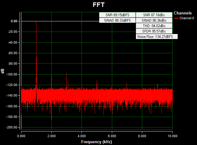
Figure 3. AC FFT for channel 0 (AIN0) using on-board isolated power, a ±10V 1kHz sine wave input signal, high-impedance input, a 20ksps sample rate, and a Blackman-Harris window.

Figure 4. DC histogram for channel 0 (AIN0) using on-board isolated power; a 0V input signal; high-impedance input; a 20ksps sample rate; 65,536 samples; a code spread of 7 LSBs with 97.57% of the codes falling within the three center LSBs; and a standard deviation of 0.693.

Figure 5. AC FFT for channel 0 (AIN0) using external power, a ±10V 1kHz sine wave input signal, high-impedance input, a 20ksps sample rate, and a Blackman-Harris window.
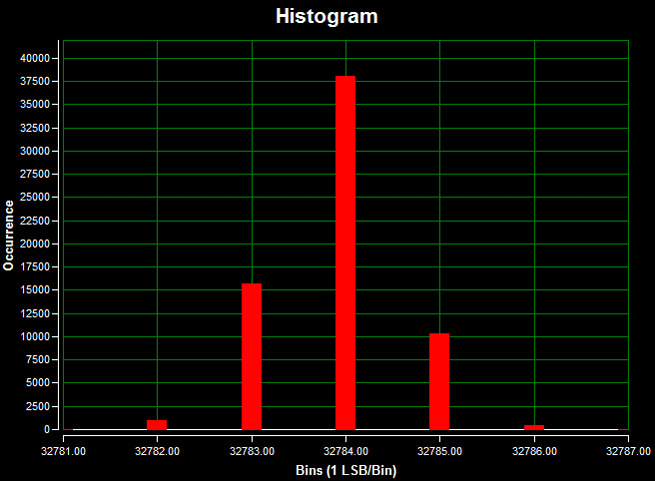
Figure 6. DC histogram for channel 0 (AIN0) using external power; a 0V input signal; high-impedance input; a 20ksps sample rate; 65,536 samples; a code spread of 7 LSBs with 97.74% of the codes falling within the three center LSBs; and a standard deviation of 0.692.
Figures 7 to 10: Channel 1 (AIN1) (PDF)