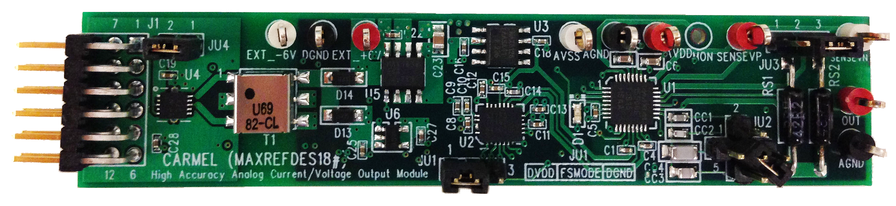
CARMEL (MAXREFDES18#):高精度模拟电流/电压输出

概述
 高清图片 (PNG) |
在PLC和DCS系统中,模拟输出电流和电压提供关键的控制和驱动功能。图1所示的Carmel (MAXREFDES18#)参考设计提供满足工业控制要求的灵活、可编程模拟输出。
MAX5316 16位高精度数/模转换器 (DAC)的带缓冲电压输出驱动MAX15500可编程模拟输出调理器的输入,后者提供各种错误报告。MAX6126超高精度电压基准为DAC和输出调理器提供基准。MAX14850实现子系统和系统控制器之间数据通信的电隔离。子系统也可选择使用MAX13253变压器驱动器和MAX1659及MAX1735低压差(LDO)线性稳压器,从而集成隔离、稳压电源。
子系统具有全部典型的双极性电流和电压输出范围以及相应子集,总不可调误差(TUE)小于0.105%。电路也提供短路和过流保护、开路检测、掉电检测、过热保护,所有这些对工业应用都至关重要。灵活的上电选项使Carmel可理想用于强大的工业控制系统。
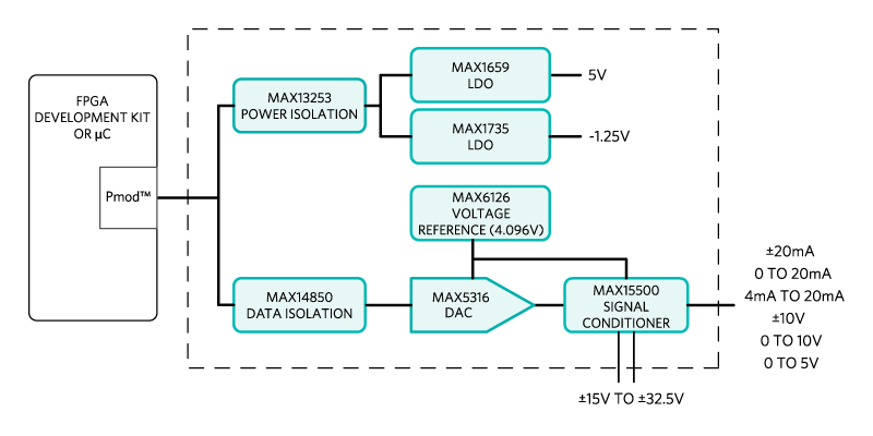
图1. Carmel子系统设计方框图。
特性 |
应用 |
|
|
竞争优势
- 灵活性
- 系统安全
- 方案尺寸小
- 低成本
详情介绍
Introduction
More detailed image (PNG) |
In PLC and DCS systems, analog output currents and voltages provide critical control and actuation functions. The Carmel (MAXREFDES18#) reference design shown in Figure 1 provides a flexible and programmable analog output that meets industrial control requirements.
The buffered voltage output from the MAX5316 16-bit, high-accuracy digital-to-analog converter (DAC) drives the input of the MAX15500, a programmable analog output conditioner with extensive error reporting. The MAX6126 ultra-high-precision voltage reference provides references for the DAC and the output conditioner. The MAX14850 galvanically isolates data communication between the subsystem and the system controller. Optionally, the subsystem also integrates an isolated and regulated power supply by using the MAX13253 transformer driver and the MAX1659 andMAX1735 low-dropout (LDO) linear regulators.
The subsystem features all typical bipolar current and voltage output ranges, and appropriate subsets, with less than 0.105% total unadjusted error (TUE). The circuit also provides short-circuit and overcurrent protection, open circuit detection, brownout detection, overtemperature protection, all of which are critical for industrial applications. Flexible power-up options make Carmel an ideal choice for robust industrial control systems.
Figure 1. The Carmel subsystem design block diagram.
Features |
Applications |
|
|
Competitive Advantages
- Flexibility
- System safety
- Small solution size
- Low cost
Detailed Description of Hardware
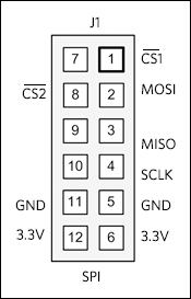 Carmel connects to Pmod-compatible field-programmable gate array (FPGA)/microcontroller development boards. Carmel requires a 3.3V supply voltage from the Pmod connector and uses the SPI pin assignments as illustrated here.
The power requirements are shown in Table 1. Note that the external AVDD and AVSS power rails are required for full system operation. The currently supported platforms and ports are shown in Table 2.
Table 1. Power Requirements for the Carmel Subsystem Reference Design
| Power Name | Jumper Shunt | Input Voltage (V) | Input Current (mA, max) |
|---|---|---|---|
| 3.3V Pmod Power Supply | JU4: 1-2 | 3.3 | 49.0 |
| AVDD | — | 15.0 to 32.5 | 25.0 |
| AVSS | — | -15.0 to -32.5 | 25.0 |
Table 2. Supported Platforms and Ports
| Supported Platforms | Ports |
|---|---|
| LX9 platform (Spartan®-6) | J5 |
| ZedBoard platform (Zynq®-7020) | JA1 |
The MAX15500 (U1) is a single-channel, low-cost, precision analog current/voltage output conditioner developed to meet the requirements of PLCs and other industrial control and automation applications. The MAX15500 operates from a ±15V to ±32.5V power-supply range.
The MAX15500 can generate both unipolar and bipolar current and voltage outputs. In current mode, the device produces currents of -1.2mA to +24mA or -24mA to +24mA. In voltage mode, the device produces voltages of -0.3V to +6V, -0.6V to +12V, or ±12V. To allow for overrange and underrange capability in unipolar mode, the transfer function of the MAX15500 is offset so that when the voltage at AIN is 5% of full scale, IOUT is 0mA and VOUT is 0V. Once VAIN attains full scale, VOUT or IOUT becomes full scale +5% or +20% depending on the state of FSMODE.
The MAX15500 protects against overcurrent and short-circuit conditions when OUT goes to ground or a voltage up to ±32.5V. The device also monitors for overtemperature and supply brownout conditions. The supply brownout threshold is programmable between ±10V and ±24V in 2V increments. The MAX15500 provides extensive error reporting of short-circuit, open-circuit, brownout, and overtemperature conditions through the SPI interface and an additional open-draininterrupt output (ERROR). The MAX15500 also includes an analog 0 to 3V output (MON) to monitor the load condition at OUT.
The MAX5316 (U2) is a high-accuracy, 16-bit, buffered voltage-output DAC. The device features ±1 LSB integral nonlinearity (INL) (max) accuracy and a ±1 LSB differential nonlinearity (DNL) (max) accuracy over the -40°C to +105°C. A separate -1.25V AVSS supply allows the output amplifier to go to 0V (GND) while maintaining full linearity performance. For lower deadband requirements, the feature-reduced MAX5216 DAC can be used instead.
The MAX6126 (U3) drives the analog output conditioner and the DAC's reference input with an ultra-high-precision 4.096V voltage reference with 0.02% initial accuracy and a 3ppm/°C maximum temperature coefficient (tempco).
The DAC’s output directly drives the conditioner’s input with no external components, making the interface simple.
The MAX13253 (U4) provides an isolated, functional insulation class power solution that accepts 3.3V and converts it to ±6V using an isolation transformer. Post-regulation is accomplished using the MAX1659 LDO (U5) for the 5V output, and the MAX1735 (U6) for the -1.25V output.
Data isolation between the subsystem and the controller is accomplished using the MAX14850 (U7) digital data isolator. The combined power and data isolation achieved is 600VRMS.
Detailed Description of Firmware for LX9 and ZedBoard Platforms
Table 2 shows the currently supported platforms and ports. Support for additional platforms may be added periodically under Firmware Files in the All Design Files section.
The Carmel firmware released for the LX9 development kit targets a Microblaze™ soft-core microcontroller placed inside a Xilinx® Spartan®-6 FPGA. The Carmel firmware also supports the ZedBoard kit and targets an ARM® Cortex®-A9 processor placed inside a Xilinx Zynq system-on-chip (SoC).
The firmware is a working example of how to initiate the system and wait for a user’s input. A user can select the output mode and type in the DAC input code. The simple process flow is shown in Figure 2. The firmware is written in C using the Xilinx software development kit (SDK) tool, which is based on the Eclipse™ open source standard. Custom Carmel-specific design functions were created utilizing the standard Xilinx XSpi core version 3.03a. The SPI clock frequency is set to 3.125MHz.

Figure 2. The Carmel firmware flowchart.
The complete source code is provided to speed up customer development. Code documentation can be found with the corresponding firmware platform files.
Quick Start
Required equipment:
- Windows® PC with two USB ports
- Carmel (MAXREFDES18#) board
- Carmel-supported platform (i.e., LX9 development kit or ZedBoard kit)
- One ±24V, 25mA minimum DC power supply
- One 750Ω, 0.25W resistor
Download, read, and carefully follow each step in the appropriate Carmel Quick Start Guide:
Carmel (MAXREFDES18#) LX9 Quick Start Guide
Carmel (MAXREFDES18#) ZedBoard Quick Start Guide
Lab Measurements
Equipment:
- Carmel (MAXREFDES18#) board
- FPGA development kit
- One 750Ω, 0.25W resistor load
- Agilent 3458A digital multimeter
- Agilent E3631A DC power supply (any ±24V, 25mA minimum DC power supply works)
- National Instruments GPIB card and cable
- Thermonics T-2800 precision temperature forcing system
- Perl script for controlling the FPGA development kit and measurement equipment
- Windows PC
INL, DNL, and total unadjusted error (TUE) are the most important specifications for PLC and other process control systems. The MAX15500 is highly flexible and configurable to meet the needs of various applications. Measurements of DNL, INL, and output error for the reference design are shown in Figure 3, Figure 4, and Figure 5, respectively. The data was taken at +25°C in the -10V to +10V voltage output mode, with 5% overrange.
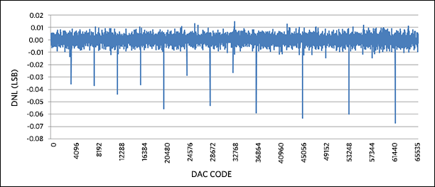
Figure 3. DNL for -10V to +10V output range, with 5% overrange.
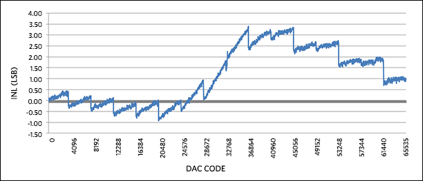
Figure 4. INL for -10V to +10V output range, with 5% overrange.
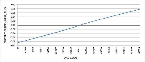
Figure 5. Output error for -10V to +10V output range, with 5% overrange.
In the case of current output, DNL, INL, and output error (without calibration) for the reference design are shown inFigure 6, Figure 7, and Figure 8, respectively. The data was taken at +25°C in the 0mA to 20mA current output mode, with 5% overrange.
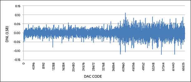
Figure 6. DNL for 0 to 20mA output range, with 5% overrange.
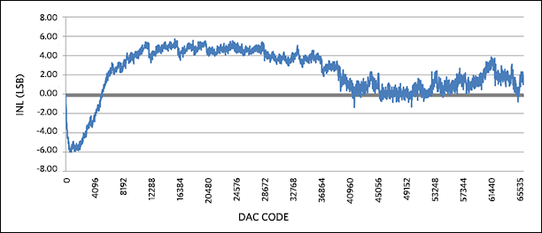
Figure 7. INL for 0 to 20mA output range, with 5% overrange.
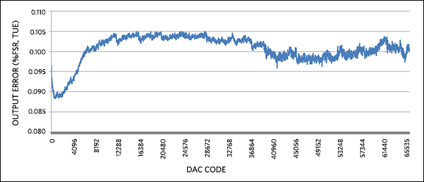
Figure 8. Output error for 0 to 20mA output range, with 5% overrange.ARM is a registered trademark and registered service mark of ARM Limited.
![]()
Cortex is a registered trademark of ARM Limited.
Eclipse is a trademark of Eclipse Foundation, Inc.
Halo is a registered trademark of Halo Electronics, Inc.
MicroBlaze is a trademark of Xilinx, Inc.
Pmod is a trademark of Digilent Inc.
Spartan is a registered trademark of Xilinx, Inc.
Windows is a registered trademark and registered service mark of Microsoft Corporation.
Xilinx is a registered trademark and registered service mark of Xilinx, Inc.
ZedBoard is a trademark of ZedBoard.org.
Zynq is a registered trademark of Xilinx, Inc.