MAXREFDES39#:通过MAX11300 PIXI实现功率放大器偏置


概述
MAXREFDES39#功率放大器(PA)偏置参考设计使用MAX11300,可用来偏置和监测射频基站系统应用中的功率放大器。本例中使用的是Infineon的 PTMA210152M-20W,但可使用任意其它功率放大器。MAX11300为射频功率放大器偏置基础设施提供高度集成的方案。设计全部使用MAX11300的模拟外设,只需要一片MAX11300即可偏置和监测2级射频功率放大器。参考设计的特性如下:
详情介绍
Introduction
The MAXREFDES39# power amplifier (PA) bias reference design uses the MAX11300, also called a programmable mixed-signal I/O (PIXI™), to bias and monitor a power amplifier for an RF base station application. In this case, an Infineon PTMA210152M-20W is used but any Power Amplifier can be used. The MAX11300 provides a highly integrated solution for the RF power amplifier biasing infrastructure. The design utilizes all of the MAX11300’s analog peripherals, while only requiring one MAX11300 device to both bias and monitor a 2-stage RF power amp. All the features of this reference design are listed below.
- Monitor, biasing, and control for frequency division duplex (FDD) and time division duplex (TDD) radio frequency (RF) power amplifiers.
- Monitoring function
- Accurate voltage and current measurement
- Current measurement through Maxim current-sense amplifier (MAX44285)
- Drain voltage and current of first- and second-stage amplifiers
- Two external and one internal temperature monitors
- Gate biasing of first-stage and second-stage amplifiers
- Control function
- Fast RF PA on/off
- Synchronized TDD function
- Efficient, adjustable drain voltage supply
- LED signaling and alarm
- Automatic control function

Figure 1. The MAXREFDES39# system block diagram.
The USB interface to the microcontroller and serial interface to the MAX11300 are digitally isolated from the main circuit through the MAX14850. The microcontroller section is powered through USB power, whereas the rest of the circuit is powered by a separate 36V DC supply. Figure 1 also shows power control and monitoring for RF PA.
Design Details
The design uses the highly configurable input/output capability of the MAX11300 to bias an Infineon PTAM210152M; 15W, two-stage, LDMOS power amp. The MAX11300 internal design as used in this PA bias reference design is shown in Figure 2. It consists of six single-ended ADCs, four DACs, two switches, and two GPOs.

Figure 2. Internal schematic of MAX11300 for PA biasing.
In Figure 2, three of the ADCs are configured for 0 to 2.5V input range for current-sense measurement and the other three are configured for 0 to 10V input range for supply voltage detection. Two of the DACs are configured to regulate MAX17503 DC-DC converter for optimal power output for the PA. The other two DACs are used to bias stage 1 and stage 2 of the PA. GPI-controlled analog switches can be used for fast switching of DAC outputs for TDD application. If fast switching is not required, these can be left connected internally or through an isolated GPIO of microcontroller (see schematic for more details).
Input power is supplied through a 36V, 150W DC power supply. MAX17503 DC-DC converters are used to regulate 15V to 28V for PA. Their main characteristics are 4.5 to 60V input range and up to 2.5A output. As mentioned above, DAC outputs regulate the FB input of these converters, as shown in Figure 3.

Figure 3. DC-DC converter circuit.
MAX44285 current-sense amplifiers (CSAs) are used to measure bias current of stage 1 and stage 2 of the PA. The CSA output range is designed to vary from 0 to 2.5V for 0 to 1A current with a 0.05Ω sensor resistor, and a gain of 50. Therefore, the ADC range of 0 to 2.5V is selected for all ADCs used to monitor current.
To measure PA’s temperature, an external diode is attached to the PA using thermal paste and connected to the MAX11300 EXT Temp 1 pins. Another diode is attached to the PA board and connected to the MAX11300 EXT Temp 2 pins, as shown in Figure 4.

Figure 4. External temperature sensor connection scheme.
Quick Start
Required equipment:
- Windows® PC with a USB port
- MAXREFDES39# Board
- 36V, 150W DC Power Supply (included in MAXREFDES39# kit)
- Temperature sensors with cables (included in MAXREFDES39# kit)
- Infineon PTMA210152M Power Amplifier Evaluation (EV) Kit (NOT included). For details, visit http://www.infineon.com/cms/en/product/rf-and-wireless-control/rf-power/cellular-2000-mhz-to-2200-mhz/PTMA+210152M+-+20+W/productType.html?productType=db3a30431ed1d7b2011f36a16c303f45
- Necessary cables to hook up the MAXREFDES39# board and power amplifier EV kit (Figure 7). In this case two red and one black 12” Banana - Banana cables and one orange and one black 12” Banana – Mini-grabber cables are used.
- An RF attenuator may also be required to be connected between the Power Amplifier kit and Spectrum Analyzer. In this case Aeroflex # 49-3-43 is used.
Steps to test the MAXREFDES39# hardware:
- Download and install the MAXREFDES39# software.
- Connect 36V power supply to the DC jack J9
- Connect the MAXREFDES39# board through mini USB cable to PC
- Once the automatic driver software installation is complete, run the software by opening its icon in the Start Menu
- Through the Configuration Tab, load the MAX11300 configuration file (MAXREFDES39#_config_file.csv) that comes with the software
- Upon visual validation, write the file to the MAX11300 device
- Through the Control / Monitor tab, read the ADCs. The results should be close to the results shown in Figure 5.

Figure 5. Screenshot of expected ADC values during initial startup of the PA bias reference design. - Change DAC voltages of PORT0 and PORT10 from 1V–9V and measure the change in voltage from 28V to 12V at V1 and V2, respectively as shown in Figure 6.

Figure 6. Screenshot of DAC values in the PA bias GUI. - If the above tests pass, then connect the Power Amplifier EV kit as shown in Figure 7.
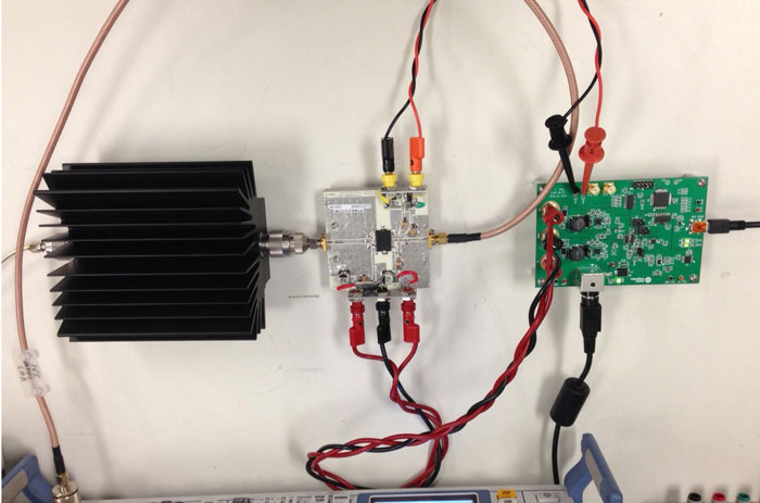
Figure 7. Connections of the MAXREFDES39# board with the PTMA210152M EV kit. - The gain of the Stage 1 and Stage 2 of the power amplifier can be adjusted through changing the DAC voltages from 2V to 3V at PORT6 and PORT14 respectively, as PTMA210152M requires this voltage range for biasing.
- The gain and offset errors can be calibrated for all DAC and ADC configured ports from the Calibration tab.
Software flow:
The software provides all required features including
- Configuration of the MAX11300 device by reading the register map file generated by the MAX11300 configuration software
- Control/monitoring feature of all analog peripherals including DAC, ADC, etc.
- Calibration of DACs and ADCs
The Configuration tab provides the option to load the MAX11300 configuration file generated by the MAX11300 configuration software. Once the file is loaded, users can view whole configuration for the device, as shown below in Figure 8. If the configuration matches Figure 8, it can be written to the MAX11300 device. This configuration can also be used with other 2-stage power amplifiers instead of PTMA210152M.

Figure 8. Screenshot of the MAXREFDES39# software - Configuration Tab.
The Control / Monitor tab provides features to set the voltages of all DAC configured ports and read the data of all ADC configured ports. Instantaneous output of ADC ports as well as averaged output can be read. The software also calculates the standard deviation of the averaged data as shown in Figure 5 and in Figure 9.

Figure 9. Screenshot of MAXREFDES39# software – Control / Monitor tab.
The Calibration tab (Figure 10) is used to calibrate the ADC and DAC gain and offset errors. The values of gain and offset error compensation are set on this tab and the effect can be seen on the ADC and DAC configured ports when data is read or written to the MAX11300 device through the Control / Monitor tab. As an example, if gain is set to 0.5 for a DAC configured on port 0 and output is set to 10V, then actual output will be 5V.

Figure 10. Screenshot of MAXREFDES39# software – Calibration tab.
Lab Measurements
The power amplifier is biased by using the MAXREDES39# board with a 2.1GHz RF input connected to the PTMA210152M EV kit. The output of the EV kit is connected to a spectrum analyzer through an RF attenuator. The power amplifier is biased through the DAC configured ports, port 6 and port 14. The spectrum analyzer result is shown in Figure 11.

Figure 11. Spectrum of power amp output when biased with the MAX11300.
The output in Figure 11 does not show any spikes added by the MAX11300 within 100kHz span, whereas the DAC update rate is 25kHz.