MAXREFDES74#:18位高精度数据采集系统


概述
MAXREFDES74#参考设计执行高速、18位、高精度数据采集,基于Maxim的前沿、高精度、低功耗数据转换器。MAXREFDES74#设计作为一个模块,适用于工业过程控制和自动化领域的高速、低功耗、高精度数据采集和控制系统,以及配电和自动化领域的高速保护系统。通过管脚兼容的16位ADC和DAC器件,例如MAX11166和MAX5316,也可测试16位数据采集系统。
MAXREFDES74#参考设计的特性包括:
- 电源和数据隔离
- 灵活、可配置的反相或同相输入方法
- 单极性或双极性输入(ADC)和输出(DAC)
MAX11156
- 18位分辨率,无失码
- 信噪比:94.4dB
- 总谐波失真:-107dB @ 1kHz
- 带缓冲的内部或外部电压基准输入
- 内部基准的温度系数为-6ppm/°C(典型值)
- 5V单电源供电
- 真正的双极性±5V输入范围
MAX5318
- 18位分辨率,无失码
- 高精度±2 LSB INL(最大值)
- 3µs稳定时间
- 用户可编程失调和增益校准
- ±0.5ppm/°C(典型值)偏移和增益漂移(全部温度范围)
- 加载/感应输出
- 50MHz SPI兼容接口,1.8V至5.5V逻辑电平
详情介绍
Introduction
The MAXREFDES74# reference design performs high-speed, 18-bit, precision data acquisition based on Maxim’s leading-edge, high-accuracy, low-power data converters. The MAXREFDES74# design works as a building block for a high-speed, low-power, high-accuracy data acquisition and control system for industrial process control and automation, and high-speed protection systems for power distribution and automation. By changing the ADC and DAC to pin-compatible 16-bit devices such as the MAX11166 and the MAX5316, a 16-bit data acquisition system can also be tested.
The MAXREFDES74# reference design features:
- Power and data isolation
- Flexible, configurable inverting or noninverting input scheme
- Unipolar or bipolar input (ADC) and output (DAC)
MAX11156
- 18-bit resolution with no missing codes
- SNR: 94.4dB
- THD: -107dB at 1kHz
- Buffered internal or external voltage reference input
- Internal reference with -6ppm/°C (typ) temperature coefficient
- Single 5V supply
- True bipolar ±5V input range
MAX5318
- 18-bit resolution with no missing codes
- High accuracy: ±2 LSB INL (max)
- 3µs settling time
- User-programmable offset and gain calibration
- ±0.5ppm/°C (typ) offset and gain drift over temperature
- Force/sense output
- 50MHz SPI-compatible interface with 1.8V to 5.5V logic
Detailed Description
The block diagram of the MAXREFDES74# board is shown in Figure 1.
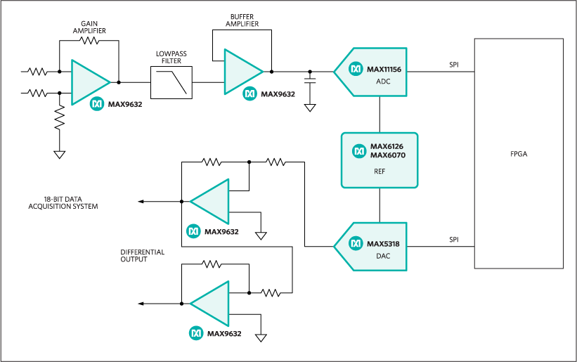
Figure 1. MAXREFDES74# block diagram.
The analog front-end consists of two user-selectable MAX9632 op amps, followed by the MAX11156. The op amps can be configured as inverting or noninverting amplifiers by jumper selectors. Both op amps work as anti-aliasing lowpass filters (LPF) and can be daisy-chained to create a second-order LPF.
The output of the MAX5318 DAC can also be configured as a positive or negative single-ended output, or as a true differential output through three MAX9632 op amps. The DAC output can also be shifted up to double the output level to 2 x VREF.
The voltage reference (VREF) for both the ADC and DAC comes from the selectable reference sources, which include the MAX6126, with 3ppm/°C, 0.02% initial accuracy VREF in an 8-pin SO package, and the MAX6070, with 6ppm/°C, 0.04% initial accuracy VREF in a 6-pin SOT23 package. The MAX11156 can use an internal VREF (default operation) or one of the external references.
The shunt positions for major ADC configurations are shown in Table 1 and Figure 2, and for the DAC output in Table 2, and a VREF connection in Table 3.
Table 1. ADC Input Configuration
| CONFIG # | ADC INPUT CONFIGURATION | INPUT CONNECTORS | SHUNT POSITIONS |
|---|---|---|---|
| 1 | Noninverting, single-ended, second-order LPF (default) | CON3: AIN0+ or (TP2 and TP8): AIN0+ and AGND | J28: 1-2 J29: 1-2 and 3-4 J32: 5-6 and 3-4 J10: 1-2 and 9-10 |
| 2 | Noninverting, differential, second-order LPF | CON3 (TP2): AIN0+ CON2 (TP1): AIN0- |
J28: Open J29: 1-2 J32: 5-6 and 3-4 J10: 1-2 and 9-10 |
| 3 | Inverting, single-ended, second-order LPF | CON2: AIN0 or (TP1 and TP8): AIN0 and AGND |
J28: 3-4 J29: 3-4 J32: 1-2 and 7-8 J10: 1-2 and 9-10 |
| 4 | Inverting, differential, second-order LPF | CON2 (TP1): AIN0- CON3 (TP2): AIN0+ |
J28: Open J29: 3-4 J32: 1-2 and 7-8 J10: 1-2 and 9-10 |
| 5 | Noninverting, single-ended, first-order LPF | CON5: AIN1 or (TP7 and TP15): AIN1 and AGND |
J29: 1-2 J32: 3-4 and 7-8 J10: 1-2 and 9-10 |
| 6 | Differential, first-order LPF | CON5 (TP7): AIN1+ CON4 (TP10): AIN1- |
J29: Open J32: 3-4 and 7-8 J10: 1-2 and 9-10 |
| 7 | Inverting, single-ended, first-order LPF | CON4: AIN1 or (TP10 and TP15): AIN1 and AGND | J29: 3-4 J32: 1-2 and 7-8 J10: 1-2 and 9-10 |
| 8 | DAC noninverting, single-ended | Use the on-board MAX5318 as input source* | J10: 3-4 and 9-10 J9: 1-2 J5: 1-2 J18: 1-2 |
| 9 | DAC inverting, single-ended | Use the on-board MAX5318 as input source* | J10: 5-6 and 9-10 J9: 1-2 J5: 1-2 J18: 1-2 |
| DAC differential | Use the on-board MAX5318 as input source* | J10: 3-4 Jump wire J10: 5-10 |
*DAC output configuration must be compliant with the ADC input range.
Table 2. DAC Output Configuration
| CONFIG # | DAC OUTPUT | SHUNT POSITIONS | OUTPUT CONNECTORS |
|---|---|---|---|
| 10 | Single ended, 0 to 3 x VREF | J9: 1-2 J5: 1-2 J18: 1-2 |
CON11: DAC_OUT+ or (TP46 and TP41): DAC_OUT+ and AGND |
| 11 | Single ended, 0 to -3 x VREF | J9: 1-2 J5: 1-2 J18: 1-2 |
CON10: DAC_OUT- or (TP18 and TP17): DAC_OUT- and AGND |
| 12 | Differential, - 3 x VREF to 3 x VREF |
J9: 1-2 J5: 1-2 J18: 1-2 |
CON11 (TP46): DAC_OUT+ CON10 (TP18): DAC_OUT- |
| 13 | Single ended, -1.5 x VREF to 1.5 x VREF (default) | J9: 3-4 J5: 1-2 J18: 1-2 |
CON11: DAC_OUT+ or (TP46 and TP41): DAC_OUT+ and AGND |
Note: Alternate connections are shown in parentheses.
Table 3. VREF Connection
| CONFIG # | VREF | SHUNT POSITIONS FOR ADC | SHUNT POSITIONS FOR DAC |
|---|---|---|---|
| 14 | Internal | J13: open (default) | — |
| 15 | External U11 (MAX6126) | J13: 2-3 | J7: 2-3 (default) |
| 16 | External U12 (MAX6070) | J13: 1-2 | J7: 1-2 |

Figure 2. Default shunt positions.
Power Supply
The MAXREFDES74# board receives power from a single DC source of 15V to 20V, 300mA through a J1 power jack. The MAX13256, H-bridge driver and transformer create an additional negative rail for +20V and -20V. The power is then rectified and regulated down to a +15V and -15V supplies for the op amps, as well as into +5V VDD and 3.3V VDDIO for VREF, ADC, and DAC. See the MAXREFDES74# schematic for details. Specific voltages may be connected to the board for each rail, see Table 4 for corresponding shunt positions.
Table 4. Power Supply to the Board
| POWER | INPUT CONNECTORS | SHUNT POSITIONS |
|---|---|---|
| Single +15V to +20V input from a wall adapter (default) | J1 | J30: 1-2 Enable U1 J15: 3-4 J16: 3-4 J17: 3-4 J24: 5-6 |
| An external ±20V | TP35 (+20V) TP30 (-20V) TP36 (Common 0V) |
J30: 2-3 Disable U1 J15: 1-2 J16: 1-2 J17: 3-4 J24: 5-6 |
| An external ±15V | TP9 (+15V) TP23 (-15V) TP22 (Common 0V) |
J30: 2-3 Disable U1 J15: 1-2 J16: 1-2 J17: 1-2 J24: 3-4 |
Mezzanine Card Operation with ZedBoard
The MAXREFDES74# board is connected to the ZedBoard through a low-pin-count FMC CON1 connector. The ZedBoard should be connected to a PC through an Ethernet port, which allows the GUI to perform different operations with full control over mezzanine card functions.
Quick Start Guide
Required Equipment
- MAXREFDES74#, 18-bit precision data acquisition board, with +15V, 1A AC-DC wall adapter or +15V DC power supply
- ZedBoard (Part Number: AES-Z7EV-7Z020-G) with +12V AC-DC wall adapter and SD card
- PC with Windows® 7 or later operating system
- Ethernet cable
- High-performance signal generator (e.g., Audio Precision 2700 series)
Procedure
The MAXREFDES74# board is fully assembled and tested. Follow the steps below to verify board operation:
- Download the latest version of the MAXREFDES74# Software GUI and MAXREFDES74# Zedboard firmware. Save the firmware and software to a temporary folder and uncompress the zip files. Store the firmware file to an SD card.
- Solder the 2-pin header on J18-3V3 of the ZedBoard. Place a shunt on the J18-3V3 header to select 3.3V I/O operation to be compatible with the MAXREFDES74# board.
- Connect the Ethernet cable from the PC to the ZedBoard and configure the Internet Protocol Version 4 (TCP/IPv4) properties in the local area connection to IP address 192.168.1.2 and subnet mask to 255.255.255.0.
- Insert the SD card with the boot file into the card slot (J12) of ZedBoard, located underneath the PCB.
- Verify the ZedBoard boot mode MIO2-6 jumpers are set to SD card mode as described in the Hardware User Guide for ZedBoard.
MIO6 GND MIO5 3V3 MIO4 3V3 MIO3 GND MIO2 GND - Turn on the power switch (SW8) of the ZedBoard to the ON position. The green power-good LED (LD13) should light and the current revision of the MAXREFDES74 firmware is displayed on the OLED (DISP1).
- Turn off the power to the ZedBoard.
- Connect the MAXREFDES74# board to the ZedBoard through the FMC connector.
- Apply power to the MAXREFDES74# board from a +15V wall adapter.
- Turn on the power to ZedBoard.
- Open the MAXREFDES74# GUI. The GUI automatically detects the network connection to the ZedBoard and displays a confirmation message. If no network connection is found, the GUI will go to demo mode.
- After the connection is established, the GUI indicates the board condition in the status bar on the bottom side of the GUI.

Figure 3. MAXREFDES74# GUI. - Verify the Clock Source, Sampling Rate, Number of Samples, and Configuration of the MAX11156 ADC, and click the Set button.
- Go to the DMM tab, select mV from the Display Units pulldown menu and click the Capture button. The reading of the MAX11156 ADC should display a small number in mV. That is the reading of the 0V (AGND) input. Make sure that all inputs are grounded by shunts on J28 and J29; see the ADC Input Configuration table, Table 1, and the MAXREFDES74# schematic.
- Go to the Scope, Histogram, and FFT tabs to verify functionality and performance of the 0V reading. Set the Sampling rate and select the Number of Samples, the Display Units, and the Average from the corresponding pulldown menu and perform a read operation by clicking the Capture button. The corresponding print screens are shown in Figure 4, Figure 5, Figure 6, and Figure 7.

Figure 4. DMM tab.
Figure 5. Scope tab.
Figure 6. Histogram tab.
Figure 7. FFT tab. - Place a J26 shunt and repeat the performance of the VREF/2 reading.
- Apply a 10kHz sine wave from an external source, e.g. Audio Precision 2700, to CON3 (AIN0+). Synchronize the external source with the MAXREFDES74# ADC by connecting CON9 (SYNC_CLK_OUT) to the REF IN input for coherent sampling. In the ADC Configuration tab, check the Sync-Out CLK (10MHz) selection box to enable the 10MHz clock output from the ZedBoard and click the Set button. Then go to the FFT tab, select Sampling Rate, Number of Samples, put desired signal frequency in the Input Signal (Hz) pulldown menu and then click the Calculate button. The GUI will calculate the coherent input signal frequency based on the coherent sampling equation. The user will then enter the adjusted signal frequency, shown in the Adjusted (Hz) box, into the external function generator. Then click the Capture button in the FFT tab.

Figure 8. Coherent sampling of a 10kHz sine wave.
Figure 9. Coherent sampling of a 1kHz sine wave.
DAC Output Set Up
- Go to the DAC configuration tab. Type in the desired DAC VOUT into the DIN (V) box and click the Set button. The software will update the DIN, OFFSET, and GAIN registers to reflect the user-desired voltage. Use an external voltmeter to check the actual DAC output on TP54, TP46, and TP18 referenced to AGND.
- The Function Generation tab allows the user to generate predefined types of signals, such as sine, square, triangle, sawtooth, or arbitrary waveforms by selecting one from the Signal Type pulldown menu. The user can enter the desired Number of Samples, the DAC Update Rate, and the Signal Frequency, and then press the Calculate button. The software will adjust the DAC update rate and calculate the adjusted signal frequency. The user also needs to adjust the Amplitude and the Offset parameter of the desired waveform.
Note: The DAC output on TP54 is in the range from 0V to VREF (4.096V), but on TP46 it can be from -1.5 x VREF (-6.1V) to 3 x VREF (+12.3V), and on TP18 from +6.1V to -12.3V, see Table 2. Alternatively, the DAC code can be entered in hex format in the DIN box and set by clicking the Write button.
By pressing the Generate button, the software calculates the necessary points and creates a lookup table (LUT) in the ZedBoard FPGA’s RAM. FPGA will loop around the LUT to generate a continuous waveform. Use an oscilloscope to check the output waveform. The output can be disabled by clicking on the Stop button.
DAC–ADC Closed-Loop Operation
The user can generate a waveform produced by the MAX5318 DAC and analyze it using the on-board MAX11156 ADC, since the DAC and ADC work independently from each other.
- Go to the Function Generator tab and generate the desired waveform, see the DAC Output Set Up for detail. Make sure that the amplitude and the offset meet the ADC input requirements.
- Set J19 shunts in position 3-4 and 9-10. The DAC_OUT+ signal is connected to the AINP input of the ADC.
- Go to the ADC Configuration tab and set the desired configuration for the ADC. Then go to the Scope tab, select the Sampling Rate, the Number of Samples, the Display Units, and the Average factor from the corresponding pulldown menu, and click the Capture button. The waveform will be captured and displayed in a scope window. Use the zoom-in feature to see the waveform.

Figure 10. Scope of the sine wave in closed-loop operation.
Windows is a registered trademark and registered service mark of Microsoft Corporation.
Xilinx is a registered trademark and registered service mark of Xilinx, Inc.
ZedBoard is a trademark of ZedBoard.org.
Zynq is a registered trademark of Xilinx, Inc.