Simulate the MAX17504EVKITB Using SIMPLIS
Introduction
The MAX17504 high-voltage, high-efficiency, synchronous step-down DC-DC converter may be evaluated using either a 3.3V output evaluation kit (MAX17504EVKITA) or a 5V output evaluation kit (MAX17504EVKITB). An additional evaluation option is to use the MAXIM_EESIM_MAX17504EVKITA.wxsch circuit file to simulate the 3.3V output EV kit circuit using the SIMPLIS/SIMetrix simulation engine. This simulation engine can be downloaded at no cost from Maxim Integrated's EE-Sim Design Tools Suite; commercial versions are also available from SIMPLIS Technologies.
Note that the design schematic can be changed within the SIMPLIS/SIMetrix tool. By changing the component values to match those of the MAX17504EVKITB and adjusting the load appropriately, the following approach could be used to simulate that EV kit as well.
Figure 1 is an image of the EE-Sim schematic MAXIM_EESIM_MAX17504EVKITA.wxsch. Since this is a switched mode power-supply (SMPS) circuit, it uses the SIMPLIS simulator rather than the SIMetrix Spice simulator that is also included with EE-Sim.
When first opened, the circuit is configured for PFM mode operation with JU2. Please refer to the EV kit documentation and the MAX17504 data sheet for more on the modes of operation.
详情介绍
Introduction
The MAX17504 high-voltage, high-efficiency, synchronous step-down DC-DC converter may be evaluated using either a 3.3V output evaluation kit (MAX17504EVKITA) or a 5V output evaluation kit (MAX17504EVKITB). An additional evaluation option is to use the MAXIM_EESIM_MAX17504EVKITA.wxsch circuit file to simulate the 3.3V output EV kit circuit using the SIMPLIS/SIMetrix simulation engine. This simulation engine can be downloaded at no cost from Maxim Integrated's EE-Sim Design Tools Suite; commercial versions are also available from SIMPLIS Technologies.
Note that the design schematic can be changed within the SIMPLIS/SIMetrix tool. By changing the component values to match those of the MAX17504EVKITB and adjusting the load appropriately, the following approach could be used to simulate that EV kit as well.
Figure 1 is an image of the EE-Sim schematic MAXIM_EESIM_MAX17504EVKITA.wxsch. Since this is a switched mode power-supply (SMPS) circuit, it uses the SIMPLIS simulator rather than the SIMetrix Spice simulator that is also included with EE-Sim.
When first opened, the circuit is configured for PFM mode operation with JU2. Please refer to the EV kit documentation and the MAX17504 data sheet for more on the modes of operation.
Setting Up the Load
LOAD1 is a test device for dynamically loading the circuit for various simulations. It is initially set up to start with a load of 1.75A then, after 1ms, it changes to 3.5A and stays at the level for 1.5ms before returning to 1.75A. The transient simulation is set to run for 4ms.
Note that some series resistance and inductance was added to the output of the 24V power supply to represent the nonidealities of a real PCB and thus to avoid unreasonably small input ripple results. Of course every PCB will be different and these parameters may need adjustment for your case.
There are detailed notes on proper operation of the simulator on the schematic. They are repeated at the end of this document.
Below are several simulation plots that were run under conditions matching those of the EV kit measurements shown in the EV kit documentation. Instructions for creating each of these simulations are provided.
AC Analysis
One of the standard simulations used to evaluate a DC-DC converter design is an AC analysis of the feedback loop. This simulation uses the "BODE" and "VAC" test devices on the schematic. For this plot, we set the ANALYSIS parameter for the LOAD to AC and AC_RSRC (the load resistance) to 0.94Ω. The notes on the schematic or at the end of this document explain how to do this. First select the load device and then right-click on it. The menu in Figure 2 will pop up.
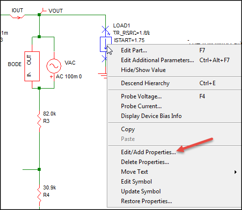 Figure 2. Changing load properties.
Click on the Edit/Add Properties item from the pop-up menu and the following window in Figure 3 will appear.
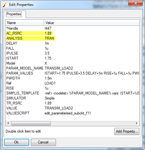 Figure 3. The Edit Properties window.
The two items that must be changed are highlighted. Double-click on ANALYSIS to get to the following Edit property window in Figure 4.
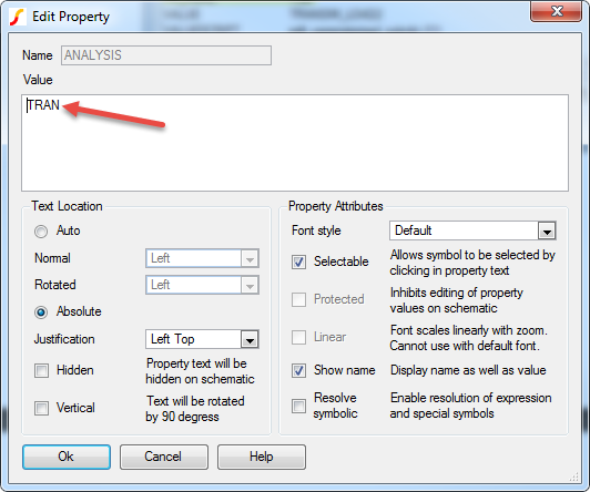 Figure 4. Edit Property window for the ANALYSIS property of the load.
This ANALYSIS property only affects how the load behaves. It has no effect on what type of simulation is run by the simulator. It has two possible states. As shown above, it is set to 'TRAN'. This tells the load to create the load pulse as defined by the various other properties. Edit this field to be 'AC' (without the quote marks). With this setting the load will simply be a fixed resistor. Click OK to save this change.
To set the resistance value for the load, double-click on AC_RSRC in the Edit Properties window. Edit the value field to be 0.94Ω for a 3.5A load. Click OK to save this change. Click OK again to close the Edit Properties window.
Now that the circuit is set up properly for an AC simulation at full load, the simulation must be told what simulation to run. The simulation type and parameters are set from the simulator menu (Figure 5): Simulator → Choose Analysis....
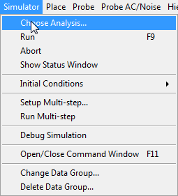 Figure 5. Getting to the Choose Analysis window.
Notice that the Transient and POP analyses as in Figure 6 are selected:
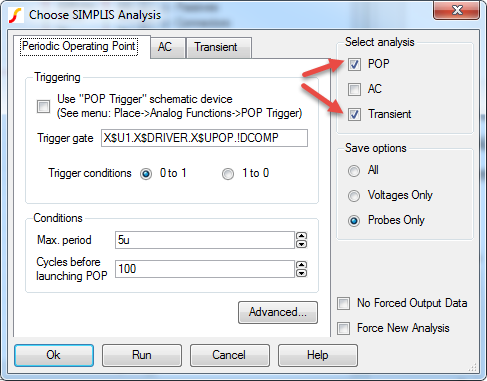 Figure 6. The Choose Analysis window.
Click on the Transient box to deselect it and the AC box to select it instead. Note that when AC is selected, the POP analysis is selected and "grayed out" shown in Figure 7. That is because a POP analysis is always needed before and AC analysis can be run. The POP analysis quickly finds the steady-state operation of the circuit from which the AC analysis can be run.
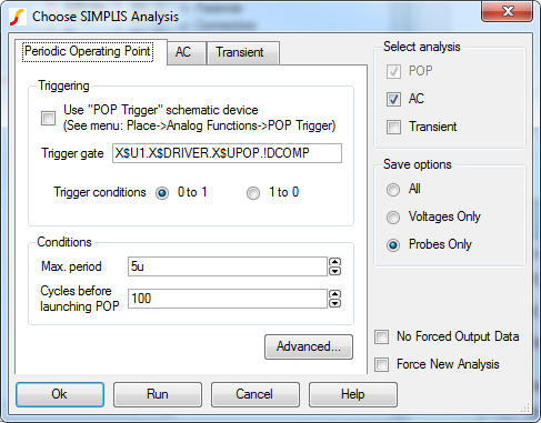 Figure 7. Selecting AC Analysis.
The POP analysis parameters have already been set up per the schematic notes. Similarly, the AC analysis parameters are set to run from 1kHz to 300kHz shown in Figure 8.
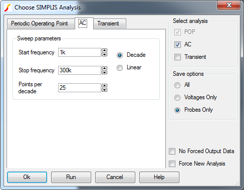 Figure 8. AC Analysis parameters.
Click the Run button. After running the AC analysis from 1kHz to 300kHz, the resulting output waveform grid, curve colors, etc. are adjusted to match the setup for Figure 6 from the EV kit documentation for easy comparison (Figure 9).
 Figure 9. Full load bode plot. Left: SIMPLIS simulation. Right: Figure 6 from the EV kit documentation.
The simulation shows unity gain cross over at 59.4kHz with 59.9° of phase margin while the EV kit measurements indicate 52.7kHz with 62.4° of phase margin. This is a 12% difference which is well within the tolerances of the inductor (30%) and output capacitors (10%).
Transient Simulation—PWM Mode
Next is a transient simulation to match Figure 7 from the EV kit documentation. This is a simulation with a load step from 0 to 1.75A and back. It is run with the MAX17504 in PWM mode. We set this up by connecting the Mode pin to ground. Double-click on the JU2 device by the Mode pin and select Position 2. Notice how the jumper has changed to connect the Mode pin to ground.
To set up the load properly, double-click on the Load symbol on the schematic and the following window in Figure 10 will pop up.
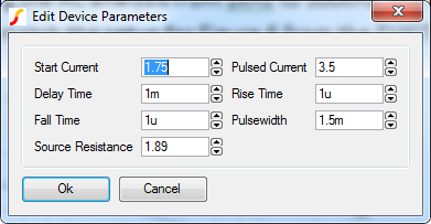 Figure 10. The Edit Device Parameters window for the load.
Edit the Device Parameters to match the conditions of Figure 7 of the EV kit documentation (shown in Figure 11).
- Start Current = 1µA
- Pulsed Current = 1.75A
- Delay time = 300µs
- Pulsewidth = 0.6ms
- Source Resistance = 3.3MΩ
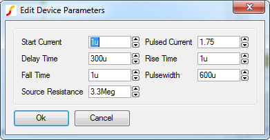 Figure 11. Setting the start current to 1µA with a 300µs delay.
The load uses a resistance, the source resistance, to set the starting current. Set this to 3.3Meg, which will result in a beginning current of about 1µA, close enough to zero. We also enter 1µA for the Start Current. This is because the schematic program has no knowledge that the voltage across the 3.3Meg resistor will be 3.3V, thus causing a current of 1µA. It has to be told what that current is so that it adds the right amount during the pulse to get to the proper Pulsed Current. In this case, we could have entered 0 for the Start Current and the pulse current would only have been off by 1µA.
At extremely low loads a POP simulation cannot reliably be run. Without the POP simulation we have to ensure that the simulation settles to steady-state before the load pulse begins. The Delay Time parameter for the Load was set to 300µs for this purpose.
We also have to change the "ANALYSIS" parameter back to 'TRAN'. Select the load and right click on it to get the menu from Figure 2 again. Double click on ANALYSIS as shown in Figure 3 and change the text in the Value box to ‘TRAN’ as shown in Figure 4. Click OK to save this change. Click OK again to close the Edit Properties window.
Setting the initial conditions of the inductor current to 0 can speed up the simulation time and make steady-state settle quicker. Double-click on the inductor and set the initial condition to 0. The notes indicate that there are three other initial conditions that can be set based on the load current to speed things up.
- Set C6's initial condition to 0 by double-clicking on C6 and changing the initial condition parameter.
- Set IC_cf (by the U1 label on top of the chip) to 0 by double-clicking on the IC_cf label and changing the value.
- Set IC_comp (near IC_cf) to 0.9.
For this case, if you leave the initial conditions unchanged, the simulation will take about 10% longer to run.
Figure 12 shows the simulation results compared to the measurements from the EV kit.
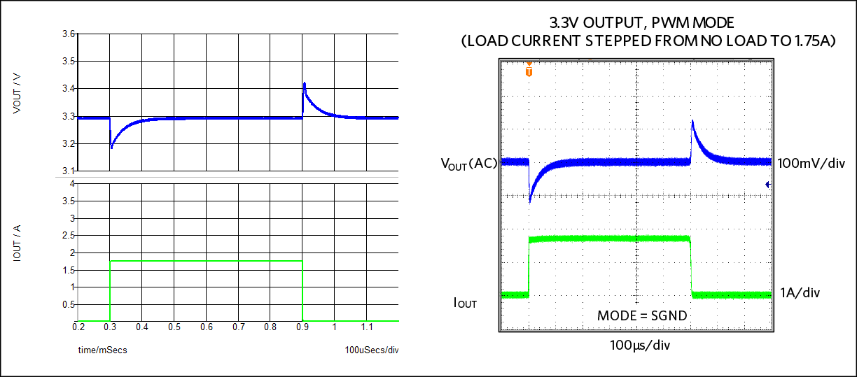 Figure 12. PWM, 0 to 1.75A load-transient simulation (left) matching Figure 7 from the EV kit documentation (right).
The output voltage transients are nearly identical to those measured for the EV kit documentation with the negative peak being about 120mV and the positive about 130mV.
Transient Simulation—PFM Mode
Figure 8 from the EV kit documentation demonstrates a similar load transient but in PFM mode. This time the starting current is 5mA and the time scale is considerably longer to clearly demonstrate what happens in this mode. First, we change the jumper on the Mode pin so that it is open, thus operating the MAX17504 in PFM mode. Next, we change the load parameters as shown in Figure 13.
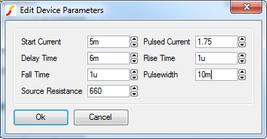 Figure 13. Setting the load for the load step in PFM mode.
Finally we set the simulator to run a transient simulation for 24ms without a POP analysis. Click on Simulator in the menu bar, then Choose Analysis… Click on the Transient tab and make sure Transient and nothing else is selected under "Select Analysis." Change the Stop time to 24m and then click on the Run button. Notice how slow the simulation runs for the 5mA load in PFM mode. When the 1.75A pulse is activated, the simulation runs much faster as the chip automatically switches to PWM mode for this relatively high load.
Again recognize that we cannot run a POP analysis so we leave time at the beginning for the circuit to settle. We see a remarkable similarity to the measured results from the EV kit documentation (Figure 14).
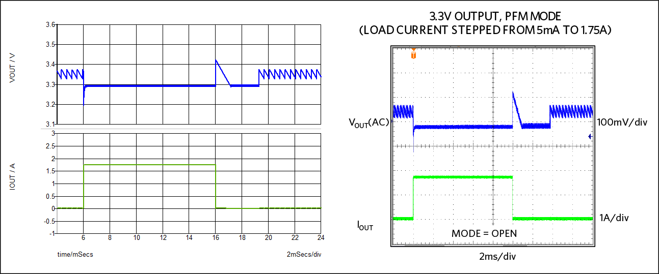 Figure 14. PFM Load step matching Figure 8 from the EV kit documentation.
Transient Simulation—DCM Mode
Next, in Figure 15, the circuit operates in DCM mode with a load transient going from 50mA to 1.75A as was done in Figure 9 of the EV kit documentation.
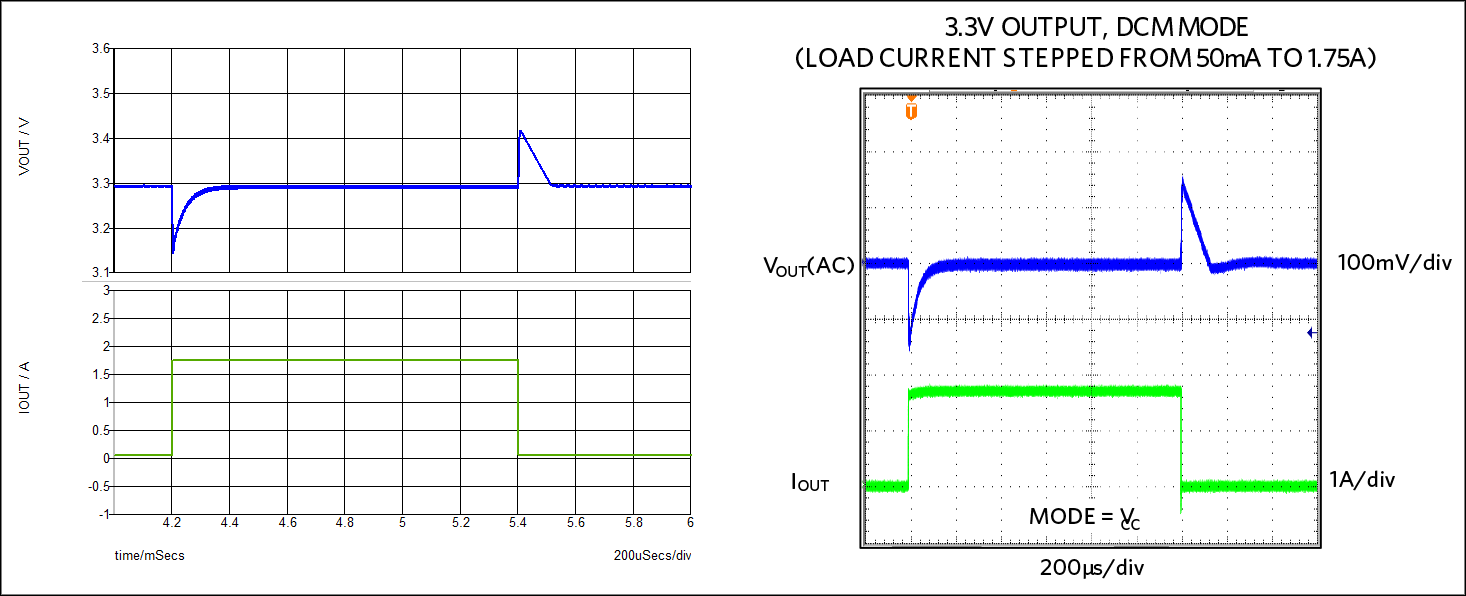 Figure 15. DCM load step simulation (left) matching Figure 9 from the EV kit documentation (right).
Again the simulated waveforms match closely with the measurements. Note that both transient voltage peaks are about 150mV. The negative one recovers with an exponential decay while the positive one has more of a sawtooth shape.
To duplicate this simulation, double click on JU2 and change it to position 1 for DCM mode. Next, double-click on the load to open its edit window. Change the Start Current to 50m and the Source Resistance to 66. Change the delay time to 4.2m and the Pulsewidth to 1.2m. Click on the OK button to close this window.
Next go to the menu bar and click on Simulator → Choose Analysis… In the Transient tab change the stop time to 6m. Then click the Run button.
Transient Simulation with POP Analysis
Figure 10 in the EV kit documentation demonstrates PWM mode with a load going from half load, 1.75A, to full load, 3.5A. This time the POP analysis is used. Along with setting the initial conditions per the schematic notes, this speeds up simulation time and eliminates the need to allow time for the circuit to settle up front. Before running the simulation change JU2 to position 2 to force PWM mode. Figure 16 shows how the load is set up.
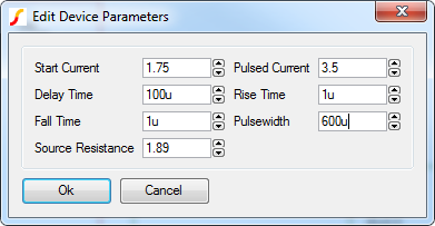 Figure 16. Setting up the load for PWM mode, half to full load pulse.
The simulator is set to run a POP analysis and then a Transient analysis for 1ms. The results are shown in Figure 17.
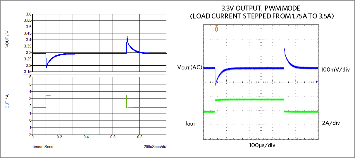 Figure 17. PWM load step simulation (left) matching Figure 10 from EV kit documentation (right).
Again there is very close agreement between this simulation and the EV kit measurements.
Notes from the MAX17504EVKITA SIMPLIS Schematic:
MAX17504 EV kit A Simulation Circuit: Circuit parameters for various simulation types
This circuit file was generated with the online EE-Sim design tool and adjusted to match the design from the MAX17504 EV kit A.
This circuit is set up to run in PFM mode for a 4ms transient simulation with a load step from 1.75A to 3.5A. The LOAD1 device is set up to provide this load step.
The BODE and VAC devices are in place to allow measuring the control loop with AC simulations.
If you want to run a different kind of simulation (AC, steady state, etc.) or change the parameters of this load step transient simulation, read the notes below.
If you are new to SIMPLIS or simulation in general, a short-cut is to use the online EE-Sim design tool to create the default design that is set up, run other types of simulations, and download the design. You can then modify that downloaded schematic for component changes or you can copy the way that simulation is set up; options from the menu item Simulator > Choose Analysis, initial conditions, LOAD1 parameters, etc.
The following are instructions for modifying the schematic and simulator settings to run different simulations yourself.
The load device has several parameters to modify for different simulations. The load acts as a resistor in parallel with a pulsed current for transient load-pulse simulations. When a load pulse is not used the load acts as a resistor.
Double-click the load for a pop-up window with editable parameters for timing and amplitude of the pulse.
1.) to 4.) Delay Time, Rise Time, Pulse Width, and Fall Time are used to set the timing of the pulsed load
5.) Source Resistance sets the lower current of the pulse waveform; Current = Vout/Source Resistance
6.) Start Current: This parameter informs the simulator what the lower current is per the prior step
7.) Pulsed Current determines the peak current of the pulsed waveform.
Each of these parameters can be edited individually by double-clicking the corresponding label next to the load.
The current set by the Source Resistance is present throughout the simulation. The load device calculates the magnitude of the added pulse as (Pulsed Current - Start Current). In order to ensure the maximum current is the same as the value entered for Pulsed Current make sure the value entered for Start Current matches the current created by the Source Resistance; = Vout/Rsource
There are two more load parameters that are used, as follows, with the 'Edit/Add Properties' menu item.
1.) Select the LOAD
2.) Right-click on LOAD
3.) Select 'Edit/Add Properties' from the pop-up menu
4.) ANALYSIS is a parameter that determines whether the load pulse is used or if the load is a resistance
4.1.) For transient simulations using the pulsed load set ANALYSIS to TRAN
4.2) For all AC simulations and transient simulations without the pulse load, set ANALYSIS to AC
5.) AC_RSRC sets the load resistance value used when ANALYSIS=AC
POP Simulation Settings. Accessible from the Simulator menu, Choose Analysis...
This is needed for AC simulations and steady-state as run online. POP can be used in PFM sometimes. If the starting load current is too low, pulse-skipping will occur and the POP analysis will fail. It is difficult to predict across all circuit parameter variations precisely at what load current this will occur. With the default load step going from a starting current of 1.75A to 3.5A and back, POP can reliably be run using PFM mode.
- Trigger Gate: X$U1.X$DRIVER.X$UPOP.!DCOMP
- Max. Period: 5u
- Cycles before launching POP: 100
- Click the Advanced button for the next two parameters:
- Convergence: 1n
- POP iteration limit: 20
Changing the Switching Frequency
To change the switching frequency, change R5 according to formula in datasheet as well as the Fsw parameter of the chip by double-clicking on the Fsw label above U1 to the desired switching frequency in kHz.
Components representing open circuits: 1GOhm Resistors, 1fF Capacitors
Components representing short circuits: 1mOhm Resistors
MAX17503/4/5 Initial Conditions
The items below with names beginning with IC_ are initial conditions of the chip. To edit any of them double click on the matching label above U1.
For AC, POP, and Transient Analyses (IOUT is the load current)
- Initial condition of C1 is VIN
- Initial condition of C2 and C3 is 5
- Initial condition of C4 is Vout
- Initial condition of C5 is -5
- Initial condition of C6 is (0.25 × Iout)
- Initial condition of L1 is Iout
- IC_RESET = IC_SSDONE = IC_EN = 5
- IC_cf = (0.25 × Iout)
- IC_comp = (0.25 × Iout) + 0.9
- IC_FB = IC_VREF = 0.9
- IC_clk = 1.78
For Startup Analysis
- Initial condition of C1 is VIN
- Initial condition of C2, C3, C4, C5, C6 is 0
- Initial condition of L1 is 0
- IC_RESET = IC_VREF = IC_SSDONE = IC_EN = 0
- IC_cf = IC_comp = IC_FB = 0
- IC_clk = 0


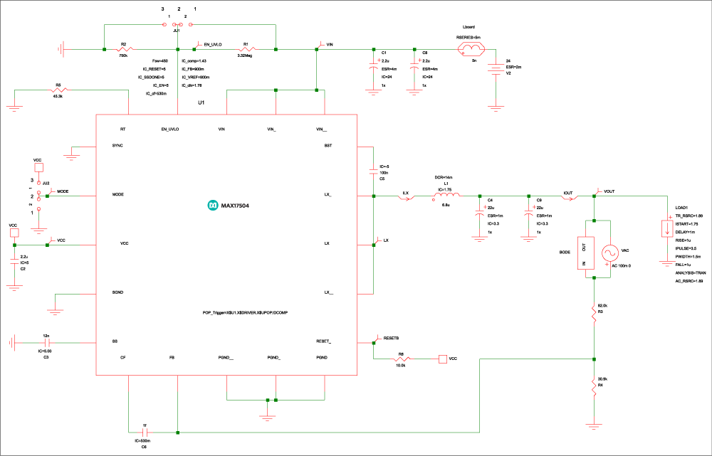 Figure 1. EE-Sim schematic.