MAXREFDES98#: Non-isolated 5V/2.5A PoE Powered Device Power Supply
为满足非隔离以太网供电(PoE)电源方案日益增长的需求,Maxim开发了创新的非隔离PoE受电设备(PD)电源方案。每款设计均经过负载及电源调整率测试,以及效率和瞬态性能测试。所有的Maxim参考设计均提供BOM、原理图、布局文件以及Gerber文件,可从“设计资源”标签页中下载。此外,备有电路板可供购买。这些电路板采用模块化结构,带有过孔插针,可直接安装电路板,加速原型开发。
MAXREFDES98#在14.0mm (0.55in) x 55.9mm (2.2in)的电路板上集成了PD控制器和降压转换器。模块支持36V至57V输入电压范围,提供5V输出电压,最大负载电流为2.5A。
为便于初始评估,Maxim也提供评估板MAXREFDES98EV#。该评估板具有RJ45连接器,可通过连接器使用供电电源快速测试。
Features
- 36V至57V输入电压
- 小巧、灵活
- 外部元件数量最少
- 在恶劣环境下工作可靠
- 12.5W输出容量
- ±3%输出精度
Applications
- 照明
- IP摄像头
- 传感器
- 非隔离以太网设备


详情介绍
Introduction
Power over Ethernet (PoE) provides power to Ethernet connected devices, through Ethernet lines, eliminating the need for connecting AC mains to the target devices. In addition to reducing cabling, PoE provides multiple advantages for many applications such as LED lighting, cameras, sensors, and additional equipment. These advantages include network management of devices, power measurement, and elimination of AC/DC circuitry.
Many PoE applications are isolated, to protect both people and systems from voltage and current transients. However, many applications do not require isolation, such as LED lighting and other equipment that is generally out of range for human touch. In these cases, eliminating the isolation circuitry further reduces cost and power dissipation at the PoE point of load. MAXREFDES98# is a unique PoE module reference design, providing 5V at 2.5A (12.5W) from a 36V to 57V input. This design can be used for evaluation, design, prototyping, and production.
MAXREFDES98# includes two function blocks: the PD controller block and the step down DC-DC power supply block. The PD controller uses the MAX5969A. The MAX5969A is an IEEE® 802.3af compliant, powered device interface controller with an integrated power MOSFET. The DC-DC power supply uses the MAX17503. The MAX17503 is a 4.5V~60V input, 2.5A output, high-efficiency synchronous step down converter with internal compensation. The entire design delivers a peak efficiency of 86% with an input of 48V.
The MAXREFDES98# features 12 through-hole pins spaced at a 2.54mm pitch standard. This modular architecture allows MAXREFDES98# to be soldered into a PCB or inserted into the MAXREFDES98EV# for evaluation.
System Diagram
 Figure 1. MAXREFDES98# reference design block diagram.
Detailed Circuit Description
The MAXREFDES98# reference design contains all the control circuitry and electric components required for designing a 36V to 57V wide-input, 5V/2.5A (12.5W) output non-isolated step down converter power supply.
On the board, there are two 6-pin connectors. Table 1 and Table 2 provide the function of each pin.
| Pin # | Name | Function |
|---|---|---|
| 1 | VA1 | Rectifier A input terminal 1 |
| 2 | VA2 | Rectifier A input terminal 2 |
| 3 | VB1 | Rectifier B input terminal 1 |
| 4 | VB2 | Rectifier B input terminal 2 |
| 5 | CP1 | PD Classification resistor terminal 1 |
| 6 | CP2 | PD Classification resistor terminal 2 |
| Pin # | Name | Function |
|---|---|---|
| 1 | VOUT | 5V output |
| 2 | VOUT | 5V output |
| 3 | GND | Ground |
| 4 | GND | Ground |
| 5 | NX | Not connected |
| 6 | RESET | Reset signal, active low |
The MAXREFDES98# circuit consists of two function blocks: the PD controller and the step down DC-DC converter.
The PD controller section employs the MAX5969A. The MAX5969A provides a complete interface for a powered device (PD), compliant with the IEEE® 802.3af standard. The MAX5969A provides the PD with a detection signature, classification signature, and an integrated isolation power switch with inrush current control. Visit the MAX5969A product folder for more information.
When the MAXREFDES98# board is connected to PoE power sourcing equipment (PSE), the MAX5969A conducts the detection and classification process according to the IEEE 802.af/at standard. The on board classification resistor R1 (619Ω) sets the power rating to class 3, a maximum of 12.95W. On the MAXREFDES98EV# board, there is one resistor place holder that can be used to change the power class. Refer to below table to select the appropriate R3 value on the MAXREFDES98EV# board.
Table 3. R3 value used to set PD classification class
| PD class | Maximum power consumed by PD | R3 value | Classification current | IEEE 802.3 af/at required classification current |
|---|---|---|---|---|
| Class 0 | 0.4W to 12.95W | open | 1.99mA | 0mA to 5mA |
| Class 1 | 0.44W to 3.94W | 143Ω | 10.8mA | 8mA to 13mA |
| Class 2 | 3.94W to 6.49W | 75Ω | 18.7mA | 16mA to 21 mA |
| Class 3 | 6.49W to 12.95W | 47Ω | 28.6mA | 25mA to 31mA |
MAX5969A provides one Power Good (PG) signal. Only after the MAX5969 internal hot-swap MOSFET switch is fully turned on, does the PG signal become active. PG is used as the signal to enable the DC-DC converter circuit. This process reduces the inrush current and the heat generated by the MAX5969 during startup.
The MAXREFDES98# reference design uses two bridge rectifiers, which make the design compatible with most PSE types. The bridge rectifiers cause power loss since there are always two diodes conducting, at the same time when the circuit is working. To improve efficiency, MAXREFDES98# uses low forward voltage Schottky bridge rectifiers. Test data shows that by using 100V/1A Schottky rectifiers (KMB110F), peak efficiency can be improved by about 1% compared to a traditional bridge rectifier such as the HD01-T.
Following the PD controller is the step down DC-DC converter. This circuit employs the MAX17503, Maxim's high efficiency, synchronous step-down DC-DC converter with internal compensation. For more specific information about the MAX17503, refer to the MAX17503 product folder. The MAX17503 circuit has been optimized for efficiency and reduction of inrush current using two different inductors. The system performs at a peak efficiency of 86% with a switching frequency to 300kHz, set with the RT resistor to 68kΩ.
For the inductor, MAXREFDES98# has been tested with the SLF12575T-150M4R7-PF from TDK and the HR320102-150 from HanRun. Test data shows these two inductors get nearly the same performance. In case you need to build your own circuit based on the MAXREFDES98# reference board, make sure the saturation current rating (ISAT) of the inductor is high enough so that saturation can occur only above the peak current-limit value of 3.7A.
The MAXREFDES98# is set to a soft-start time to 3.2ms. A soft-start reduces the inrush current from the PSE. Figure 3 shows the soft-start waveform. The yellow trace is the enable signal (PG) from the MAX5969A, and the blue trace is the output voltage from the MAX17503.
 Figure 3. Soft-start feature.
MAXREFDES98# reserves one RESET output pin (Pin 6 of J2, as described in table 2), which can be connected to the RESET pin of a microcontroller. This pin is open drain output, so users can OR (negative logic) it with another open drain signal, such as a watch dog circuit reset output, or manual reset switch. During the soft start phase, the RESET pin stays low. It goes high 3.4ms after the output voltage exceeds 4.75V. The blue trace in Figure 4 is the RESET signal, captured with an external 10kΩ resistor pulled up to VOUT. The yellow trace is the output voltage trace.
 Figure 4. RESET goes high 3.4ms after VOUT exceeds 4.75V.
Quick Start
Required equipment:
- MAXREFDES98# board
- MAXREFDES98EV# board
- RJ45 cable and one PSE RJ45 socket capable of delivering PoE, or one DC power supply adjustable to 57V
- One electronic load
- One voltmeter
Procedure
The MAXREFDES98# board is fully assembled and tested. Use the following steps to verify board operation.
- Insert the MAXREFDES98# board into the MAXREFDES98EV# board, as shown in Figure 5.
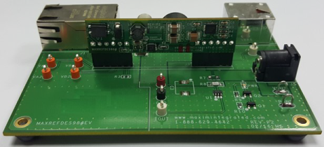 Figure 5. MAXREFDES98# connected to the MAXREFDES98EV#.
 - Insert one end of the RJ45 cable to the PSE RJ45 socket, then insert the other end to J1 on MAXREFDES98EV# board, as shown in Figure 6. The "PWR" LED on right bottom corner should light up continuously or flash slowly, depending on the PSE.
In case the "PWM" LED does not light up, the RJ45 socket likely does not have the POE feature. In this case, connect the power supply (37V~57V) to VA1/VA2, or VB1/VB2. There is no polarity requirement when the power is connected, since there are bridge rectifiers following these connectors. When the power supply is turned on, the "PWM" LED should light up continuously.
 Figure 6. When the MAXREFDES98# board works, the PWR LED on the MAXREFDES98EV# board lights up.
 - Connect the VOUT and PGND terminals on the MAXREFDES98# board to the electronic load.
- Set the electronic load to a constant current up to 2.5A.
- Connect the voltmeter to the VDC and GND, to verify the output voltage reading is 5V ±0.15V.
- Set the electronic load to "short," and turn off the PWR LED. When the "short" is released, the PWR led should light up again, and the voltage should read 5V ±0.15V.
On the MAXREFDES98EV# board, a current sense amplifier, MAX9643, measures the output current of the MAXREFDES98# board, and similar boards, such as the MAXREFDES108#. To get the actual current, divide the voltage measured by 1.6. For example, if IOUT is measured at 1.6V, the actual current drawn from MAXREFDES98# board is 1A. The IOUT is designed to measure steady state current. If it is used to capture the transient current waveform, there will be distortion on the waveform due to MAX9643's signal bandwidth and pulse response. For more information, refer to the MAX9643 data sheet. Figure 7 shows the error curve of the current measurement circuit. Error increases as measured current decreases, as is consistent with any current measuring system.
.") Figure 7. Current error of the current measurement circuit (tested on 5 samples).
Figure 7. Current error of the current measurement circuit (tested on 5 samples).
Lab Measurements Data
The MAXREFDES98# design was verified and tested under the full input range and different output load conditions.
Power efficiency vs. load current
MAXREFDES98# performs with high efficiency, across a range of input voltages. Peak efficiency is 86%, and efficiency is high across a wide output current range.
 Figure 8. Power efficiency vs. load current.
Load regulation:
Load regulation (Figure 9) was measured for input voltages of 40V, 48V, and 57V. The output voltage remains well regulated across the range of output current, deviating by less than 1.5%. Line regulation (Figure 10) is completely solid across the entire range of input voltages. Output ripple was measured at 5mA output (Figure 11) and is less than 100mV. At a current output of 2.5A, output ripple is also less than 100mV (Figure 12). Transient responses were measured from 5mA to 1000mA and back (Figure 13) and from 1500mA to 2500mA and back (Figure 14). In both cases, system response is around 100mV.
 Figure 9. Load regulation.
 Figure 10. Line regulation when output current is 1A.
 Figure 11. Output ripple at 5mA load.
.") Figure 12. Output ripple at full load (2500mA).
Figure 12. Output ripple at full load (2500mA).
 Figure 13. Load transient response when load steps between 5mA and 1000mA.
 Figure 14. Load transient response when load steps between 1500mA and 2500mA.
IEEE is a registered service mark of the Institute of Electrical and Electronics Engineers, Inc.