MAXREFDES113#: Isolated 24V to 12V 20W Power Supply
Maxim的电源专家设计和建造了一系列隔离型工业电源参考设计,其中每款电源将24V高效转换为各种功率水平的电压轨。每种电源轨都采用全球范围内多家厂商可提供的变压器进行隔离,有助于快速、便捷地选择变压器。每款设计均经过负载及电源调整率测试,以及效率和瞬态性能测试。与所有Maxim参考设计一样,设计资源选项卡提供BOM、原理图、布局文件以及Gerber文件。此外,备有电路板可供购买;大多数电路板具有过孔引脚,可立即布置电路板、加快初始产品的开发。
MAXREFDES113#是一种高效的反激式结构24 V输入、12V/20W 输出(1.6A)的电源设计。设计采用MAX17596峰值电流模式转换器,具有灵活的开关频率。整个电路安装在20mm × 35mm电路板上。
特性
- 功能隔离
- 小巧、灵活
- 外部元件数量最少
- 在恶劣环境下工作可靠
- 12V 1.6A,20%过载电流范围
- ±5%输出精度
应用
- 工业控制和自动化
- 过程控制l
- PLC
- 电信和数据通信电源


详情介绍
Introduction
Isolated power supplies provide reliable power regulation for a variety of applications. Transformer selection is often the most difficult step in isolated power design. The MAXREFDES113# is a compact 24V input flyback converter module that features 12V at 1.6A output. Multiple transformers (Halo Electronics TGSP-P153EP13LF, Wurth Electronics 750316112r01, HanRun HR051441, and Sumida 13324-T115) have been qualified for this design, simplifying the process of transformer selection. In addition, through-hole pins on the bottom side of the module allow for quick and easy integration of this power converter into the main system. Pins are 15.24mm (0.6in) from power to ground, and 27.94mm (1.1in) from the input side to the output side.
The MAX17596 is a peak-current-mode controller for design of wide input-voltage flyback and boost regulators. The reference design operates over a 17V to 36V input voltage range, and provides up to 1.6A (plus 20% overhead) at 12V output. The MAX17596 has an internal amplifier with 1% accurate reference, eliminating the need for an external reference. The switching frequency is programmable from 100kHz to 1MHz with an accuracy of 8%, allowing optimization of magnetic and filter components, resulting in compact and cost-effective power conversion. This design is set to switch at 200kHz. For EMI-sensitive applications, the MAX17596 incorporates a programmable frequency dithering scheme, enabling low-EMI spread-spectrum operation.
The input undervoltage lockout (EN/UVLO) is provided for programming the input-supply start voltage (set to 17V in the design), and to ensure proper operation during brownout conditions. The EN/UVLO input is also used to turn on/off the IC. The overvoltage input (OVI) protection scheme is provided to make sure that the controller shuts down when the input supply exceeds its maximum allowed value (set to 36V in the design).
A capacitor is connected to the SS pin to program the soft-start period hence reduces the input inrush current during startup. Hiccup-mode overcurrent protection and thermal shutdown are provided to minimize dissipation in overcurrent and overtemperature fault conditions.
The reference design delivers a peak efficiency of 87% with the supplied components when the input is 24V. This general-purpose power solution can be used in many different types of power applications, such as programmable logic controllers (PLC), industrial process control, industrial sensors, telecom power supplies, isolated battery chargers, servers, and embedded computing.
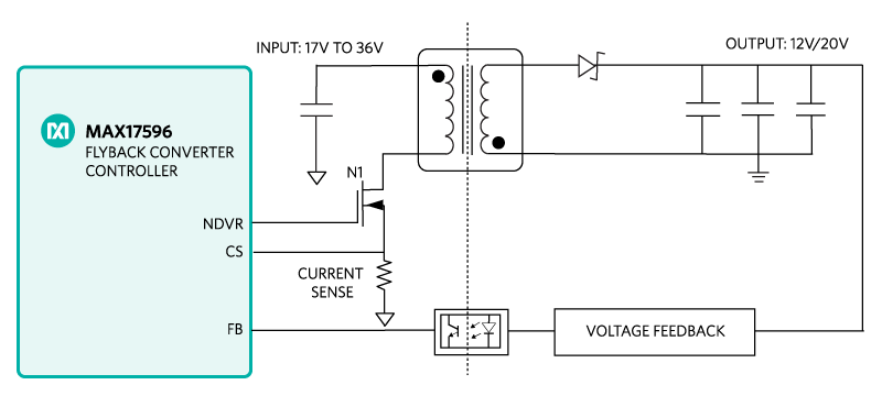 Figure 1. The MAXREFDES113# reference design block diagram.
Detailed Circuit Description
The MAXREFDES113# reference design contains all the control circuitry and electric components required for designing a 17V to 36V wide-input, 12V, 20W output isolated flyback converter power supply. When the MOSFET is turned on, the current flows through the primary winding of the transformer, which stores the energy. The CS-pin input and the current sense resistor set the peak current limit and provide overcurrent protection. When the MOSFET is turned off, the energy stored in the primary side transfers to the secondary side.
The secondary side of the circuit consists of a diode, and a few output capacitors. When the MOSFET on the primary side is off, the transformer pushes the current to the load at the output and the remaining energy is stored in the output capacitors. When the MOSFET is on, the diode prevents the current flow back into the transformer and discharges the output capacitors.
The feedback network is typical of most isolated flyback converters. It is constructed using a TL431 programmable shunt regulator, a 3000V isolation opto-coupler, and other RC components.
Startup Voltage and Input Overvoltage Protection Setting (EN/UVLO, OVI)
The EN/UVLO pin in the MAX17596 serves as an enable/disable input, as well as an accurate programmable undervoltage lockout (UVLO) pin. The MAX17596 does not begin startup operations unless the EN/UVLO pin voltage exceeds 1.21V (typ). The MAX17596 turns off if the EN/UVLO pin voltage falls below 1.15V (typ). A resistor divider from the input DC bus to ground can be used to divide down and apply a fraction of the input DC voltage to the EN/ UVLO pin. The values of the resistor divider can be selected so that the EN/UVLO-pin voltage exceeds the 1.21V (typ) turn-on threshold at the desired input DC bus voltage. The same resistor divider can be modified with an additional resistor, ROVI, to implement overvoltage input protection in addition to the EN/UVLO functionality. When the voltage at the OVI pin exceeds 1.21V (typ), the MAX17596 stops switching. Switching resumes with soft-start operation, only if the voltage at the OVI pin falls below 1.15V (typ). For the expected values of the startup DC input voltage (VSTART) and overvoltage-input protection voltage (VOVI), the resistor values for the divider can be calculated as follows:
VSTART = (R5 + R6 + R7)/(R6 + R7) × 1.21 (V)
VOVI = (R5 + R6 + R7)/R7 × 1.21 (V)
If R5 = 280kΩ, R6 = 13kΩ, and R7 = 10kΩ, then:
VSTART = 15.94V, VOVI = 36.66V.
Quick Start
Required equipment
- MAXREFDES113# board
- One 24V DC power supply
- One electronic load
- 1 voltmeter
- 1 ammeter
Procedure
The MAXREFDES113# board is fully assembled and tested. Use the following steps to verify board operation.
- Turn off the power supply.
- Connect the positive terminal of the power supply to the VIN pin of the MAXREFDES113# board.
- Connect the negative terminal of the power supply to the PGND pin of the MAXREFDES113# board.
- Connect the VOUT connector of the MAXREFDES113# board to the positive terminal of the electronic load.
- Connect the negative terminal of the electronic load to the positive terminal of the ammeter.
- Connect the negative terminal of the ammeter to the GNDO connector of the MAXREFDES113# board.
- Connect the voltmeter across the VOUT and the GNDO connectors of the MAXREFDES113# board.
- Turn on the power supply.
- Set the electronic load to a constant current between 0mA to 1.6A.
- Verify the second voltmeter reading is 12V ±0.6V.
Lab Measurements
The MAXREFDES113# design was verified and tested under full input range and different output load conditions.
The power efficiency vs. load current is illustrated in Figure 2.
 Figure 2. Power efficiency vs. load current.
Figure 3 displays the output ripple at full load when the input is 24V.
 Figure 3. Output ripple at 800mA load, 12VOUT.
Figure 4 displays the load transient response when the load is stepped from 5mA to 640mA, and then dropped back to 5mA again. The input is 24V and output is 12V.
 Figure 4. Transient response when load steps from 5mA to 640mA.
Figure 5 shows the load transient response when the load is stepped from 960mA to 1600mA, and then dropped back to 960mA again. The input is 24V, and the output is 12V.
 Figure 5. Transient response when load steps from 960mA to 1600mA.
Ordering Information
| PART NUMBER | TRANSFORMER VENDOR | TRANSFORMER PART NUMBER |
|---|---|---|
| MAXREFDES113A# | Wurth | 750316112r01 |
| MAXREFDES113B# | Sumida | 13324-T115 |
| MAXREFDES113C# | Hanrun | HR051441 |
| MAXREFDES113D# | Halo | TGSP-P153EP13LF |