MAXREFDES128#: No-Opto Isolated, PoE, 48V to 5V, 12.5W Flyback Power Supply
To meet the increasing demands for isolated Power over Ethernet (PoE) power solutions, Maxim’s power supply experts have developed innovative, isolated, PoE, powered device (PD) power solutions. These isolated PoE power solutions efficiently convert high voltage PoE power into 5V and 12V outputs, respectively. Each design was tested for load and line regulation, as well as efficiency and transient performance. These boards feature a module architecture, with through-hole pins for immediate board placement and accelerated prototyping.
The MAXREFDES128# combines the PD controller and an efficient no-opto flyback topology with 48V input and a 5V output at 12.5W of power (2.5A). The design features the MAX5969A (powered device interface controller with integrated power MOSFET), MAX17690 (a peak-current-mode converter with flexible switching frequency), and the MAX17606 (a secondary-side MOSFET driver for flyback converter). This entire circuit fits on a 25.4mm (1in) x 64.8mm (2.55in) board.
As with all Maxim reference designs, the BOM, schematics, layout files, and Gerber files can be found on the Design Resources tab.


Features
- 36V to 57V input voltage
- Compact and flexible
- Minimal external components
- Robust operation in adverse environments
- 12.5W output capacity
- ±3% output accuracy
Applications
- Lighting
- IP cameras
- Sensors
- Isolated Ethernet equipment
详情介绍
Introduction
Power over Ethernet (PoE) provides power to Ethernet-connected devices, through Ethernet lines, eliminating the need for connecting AC mains to the target devices. In addition to reducing cabling, PoE provides multiple advantages including network management of devices, power measurement, and elimination of AC-DC circuitry for many applications like LED lighting, cameras, sensors, and additional equipment.
Many PoE applications are isolated. Isolated power supplies provide reliable power regulation for a variety of applications. The MAXREFDES128# (Figure 1) is a PoE module reference design, providing 5V at 2.5A (12.5W) from a 36V to 57V input. This design can be used for evaluation, design, prototyping, and production. The MAXREFDES128# includes two function blocks: the powered device (PD) controller block and the no-opto flyback converter block. The PD controller uses the MAX5969A. The MAX5969A is an IEEE® 802.3af/at-compliant, PD interface controller with an integrated power MOSFET. The no-opto flyback converter block uses the MAX17690 and the MAX17606.The MAX17690 is a no-opto peak-current-mode controller for design of wide input-voltage flyback and boost regulators. The reference design operates over a 36V to 57V input voltage range, and provides up to 2.5A at 5V output. The switching frequency is programmable from 50kHz to 250kHz, allowing optimization of filter components, and thereby resulting in compact and cost-effective power conversion. This design is set to switch at 100kHz. An optocoupler or tertiary winding is not needed to derive feedback signal across isolation boundary.
The input undervoltage lockout (EN/UVLO) is provided for programming the input-supply start voltage (set to 36V in the design) and to ensure proper operation during brownout conditions. The EN/UVLO input is also used to turn on/off the IC. The overvoltage input (OVI) protection scheme is provided to ensure the controller shuts down when the input supply exceeds its maximum allowed value (set to 57V in the design).
A capacitor is connected to the SS pin to program the soft-start period, reducing the input inrush current during startup. Hiccup-mode overcurrent protection and thermal shutdown are provided to minimize dissipation in overcurrent and overtemperature fault conditions.
The MAX17606 is the MOSFET driver. By replacing the secondary diode with a MOSFET, the MAX17606 improves efficiency and makes the thermal management easier.
The reference design delivers a peak efficiency of 85% with the supplied components when the input is 48V. This isolated PoE power module can be used in many types of power applications.
System Diagram
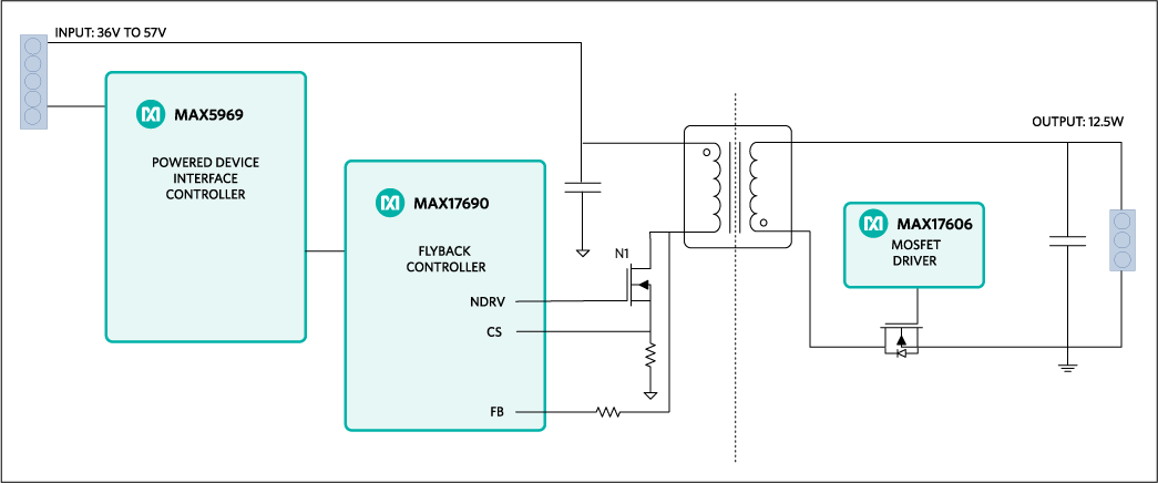 Figure 1. The MAXREFDES128# reference design block diagram.
Detailed Circuit Description
The MAXREFDES128# reference design contains all the control circuitry and electric components required for designing a 36V to 57V wide input, 5V, 12.5W output, isolated flyback converter power supply. There are two 6-pin connectors on the board. Table 1 and Table 2 provide the pin functions for J1 and J2, respectively. See Figure 2 for the board view.
Table 1. J1 Pin Description
| Pin # | Name | Function |
|---|---|---|
| 1 | VA1 | Rectifier A input terminal 1 |
| 2 | VA2 | Rectifier A input terminal 2 |
| 3 | VB1 | Rectifier B input terminal 1 |
| 4 | VB2 | Rectifier B input terminal 2 |
| 5 | CP1 | PD Classification resistor terminal 1 |
| 6 | CP2 | PD Classification resistor terminal 2 |
Table 2. J2 Pin Description
| Pin # | Name | Function |
|---|---|---|
| 1, 2 | VOUT | 5V output |
| 3, 4 | GND | Ground |
| 5, 6 | NC | Not connected |
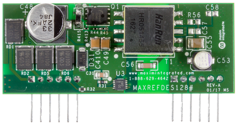 Figure 2. MAXREFDES128# board view.
The MAXREFDES128# circuit consists of two function blocks: the PD controller and the no-opto flyback DC-DC converter.
The PD controller section employs the MAX5969A. The MAX5969A provides a complete interface for a PD compliant with the IEEE 802.3af/at standard. The MAX5969A provides the PD with a detection signature, classification signature, and an integrated isolation power switch with inrush current control. When the MAXREFDES128# board is connected to PoE power-sourcing equipment (PSE), the MAX5969A conducts the detection and classification process according to the IEEE 802.af/at standard. The on-board classification resistor R32 (619) sets the power rating to class 3, a maximum of 12.95W. To test the MAXREFDES128#, you must also use another reference design, the MAXREFDES98#EV board. On the MAXREFDES98#EV board, there is one resistor placeholder (R3) that can be used to change the power class. See Table 3 to select the appropriate R3 value on the MAXREFDES98#EV board.
Table 3. R3 Value Used to Set PD Classification Class
| PD class |
Maximum power consumed by PD (W) | R3 value () | Classification current (mA) | IEEE 802.3 af/at required classification current (mA) |
|---|---|---|---|---|
| Class 0 | 0.44 to 12.95 | open | 1.99 | 0 to 5 |
| Class 1 | 0.44 to 3.94 | 143 | 10.8 | 8 to 13 |
| Class 2 | 3.94 to 6.49 | 75 | 18.7 | 16 to 21 |
| Class 3 | 6.49 to 12.95 | 47 | 28.6 | 25 to 31 |
The MAX5969A provides one power-good (PG) signal. The PG signal becomes active only after the MAX5969A internal hot-swap MOSFET switch is fully turned on. PG is used as the signal to enable the DC-DC converter circuit. This process reduces the inrush current and the heat generated by the MAX5969A during startup.
The MAXREFDES128# reference design uses two rectifiers that make the design compatible with most PSE types. The bridge rectifiers cause power loss since there are always two diodes conducting, at the same time, when the circuit is working.
Following the PD controller is the no-opto flyback DC-DC converter. This circuit employs the MAX17690, Maxim’s 60V, no-opto isolated flyback controller. The MAX17690 is a peak current mode, fixed-frequency switching controller specifically designed for the isolated flyback topology operating in Discontinuous Conduction Mode (DCM). The system performs at a peak efficiency of 85% with a switching frequency to 100kHz.
When the primary-side MOSFET is turned on, the current flows through the primary winding of the transformer and stores the energy. The CS pin input and the current-sense resistor set the peak current limit and provide overcurrent protection. When the MOSFET is tuned off, the energy stored in the primary side is transferred to the secondary side. The MAX17690 samples the output voltage by sensing the voltage of the transformer on the primary side.
For the transformer, the MAXREFDES128# has been tested with the HR051455 from HanRun. In case you need to build your own circuit based on the MAXREFDES128# reference board, you can calculate your own transformer with assistance from Application Note 5504.
The MAXREFDES128# also uses the MAX17606 in the secondary-side of the circuit as a secondary-side synchronous MOSFET driver. The secondary MOSFET is there to emulate the diode in a typical flyback converter. The MAX17606 senses the voltage at the drain pin of the MOSFET to determine the timing of turning on/off the MOSFET. When the MOSFET on the primary side is off and the drain voltage of the MOSFET on the secondary side becomes less than -100mV, the MAX17606 turns on the MOSFET and the transformer pushes the current to the load at the output, and the remaining energy is stored in the output capacitors. When the MOSFET is on and the drain voltage of the MOSFET on the secondary side becomes more than 30mA, the MAX17606 turns off the MOSFET to prevent the current flow back into the transformer and discharges the output capacitors.
Startup Voltage and Input Overvoltage Protection Setting (EN/UVLO, OVI)
The MAXREFDES128# is set to a 5ms soft-start time. A soft-start reduces the inrush current from the PSE. The MAX17690’s EN/UVLO pin can be connected to a resistive divider between the input supply. The MAX17690 starts switching when the voltage at the EN/UVLO pin exceeds 1.215V and stops switching when the voltage at the EN/UVLO pin falls below 1.1V.
The MAX17690’s OVI pin operates similarly to the EN/UVLO pin. The MAX17690 stops switching when the voltage at the OVI pin exceeds 1.215V and resumes switching when the voltage at the OVI pin falls below 1.1V. The MAXREFDES128# uses R1, R41, and R42 to build the resistive divider for the EN/UVLO pin and OVI pin.
Quick Start Guide
Required Equipment:
- MAXREFDES128# board
- MAXREFDES98#EV board
- RJ45 cable and one PSE RJ45 socket, capable of delivering PoE or DC power supply adjustable to 57V
- One electronic load
- One multimeter
Procedure
The MAXREFDES128# board is fully assembled and tested. Use the following steps to verify board operation.
- Insert MAXREFDES128# board into the MAXREFDES98#EV board, as shown in Figure 3.
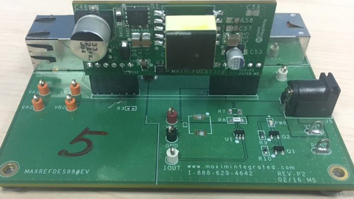 Figure 3. MAXREFDES128# connected to the MAXREFDES98#EV board.
 - Insert one end of the RJ45 cable to the PSE RJ45 socket, and insert the other end to J1 on the MAXREFDES98#EV board, as shown in Figure 4. The PWR LED on the right bottom corner should light up continuously or flash slowly, depending on the PSE.
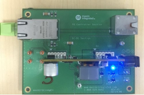 Figure 4. When the MAXREFDES128# board works, the PWR LED on the MAXREFDES98#EV board lights up.
 - Connect the VOUT and PGND terminals on the MAXREFDES98#EV board to the electronic load.
- Set the electronic load to a constant current up to 2.5A. Connect the voltmeter to the VDC and GND to verify the output voltage reading is 5V+/-0.15V.
On the MAXREFDES98#EV board, a current-sense amplifier (MAX9643) measures the output current of the MAXREFDES128# board. To get the actual current, divide the voltage measured by 1.6. For example, if IOUT is measured at 1.6V, the actual current drawn from the MAXREFDES128# board is 1A. The IOUT is designed to measure steady-state current. If it is used to capture the transient current waveform, there will be distortion on the waveform due to MAX9643’s signal bandwidth and pulse response. Figure 5 shows the error curve of the current measurement circuit. Error increases as measured current decreases, as is consistent with any current measuring system.
.") Figure 5. Current error of the current measurement circuit (tested on five samples).
Figure 5. Current error of the current measurement circuit (tested on five samples).
Lab Measurements
The MAXREFDES128# design was verified and tested under the full input range and different output load conditions.
Power Efficiency vs. Load Current
Figure 6 shows the power efficiency vs. load current with peak efficiency at 88%.
 Figure 6. Power efficiency vs. load current.
Load Regulation
Load regulation (Figure 7) was measured for input voltages of 36V, 48V, and 57V. The output voltage remains well-regulated across the output current range, deviating by less than 2%. Line regulation (Figure 8) is completely solid across the entire range of input voltages. At a current output of 2.5A, output ripple is also less than 100mV (Figure 9). Transient responses were measured from 5mA to 1000mA and back (Figure 10), and from 1500mA to 2500mA and back (Figure 11). In both cases, system response is approximately 100mV.
 Figure 7. Load regulation.
 Figure 8. Line regulation when output current is 1.25A.
 Figure 9. Output ripple at full load.
Figure 10 displays the load-transient response when the load is stepped from 50mA to 1A, and then dropped back to 50mA again. The input is 48V and the output is 5V.
 Figure 10. Load transient response when load steps between 5mA and 1000mA.
Figure 11 shows the load-transient response when the load is stepped from 1.5A to 2.5A, and then dropped back to 1.5A again. The input is 48V, and the output is 5V.
 Figure 11. Load transient response when load steps between 1500mA and 2500mA.
Ordering Information
| Part number | Transformer vendor | Transformer part number |
|---|---|---|
| MAXREFDES128# | HanRun | HR051455 |
IEEE is a registered service mark of the Institute of Electrical and Electronics Engineers, Inc.