CN0399
Battery or USB Powered 9 kHz to 6 GHz RMS Power Measurement System
详情介绍


概览
设计资源
评估硬件
产品型号带"Z"表示符合RoHS标准。评估此电路需要下列选中的电路板
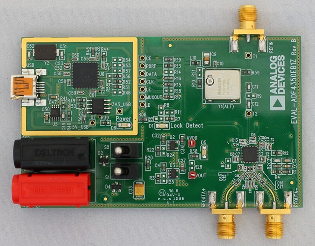
- EVAL-ADF4350EB1Z ($175.00) ADF4350 evaluation board used to evaluate this circuit. Please see "Circuit Evaluation & Test" section for set up information.
驱动/参考代码
Software such as C code and/or FPGA code, used to communicate with component's digital interface.
优势和特点
- 宽带直接变频发射机
- 可在69 MHz至2.2 GHz之间工作
电路功能与优势
本电路为宽带直接变频发射机模拟部分的完整实施方案(模拟基带输入、RF输出)。通过使用锁相环(PLL)和宽带集成电压控制振荡器(VCO),本电路支持68.75 MHz至2.2 GHz范围内的RF频率。与使用1分频LO级的调制器(如
CN-0134所述)不同,本电路不需要对LO进行谐波滤波。为实现最佳性能,只要求调制器的LO输入采用差分方式驱动。
ADF4350 提供差分RF输出,因此非常适合这种调制器。低噪声LDO确保电源管理方案对相位噪声和误差矢量幅度(EVM)无不利影响。这种器件组合可以提供68.75 MHz至2.2 GHz频率范围内业界领先的直接变频发射机性能。对于2.2 GHz以上的频率,建议使用CN-0134所介绍的1分频调制器。

图1. 直接变频发射机(原理示意图:未显示去耦和所有连接)
电路描述
图1所示电路使用完全集成的小数N分频PLL ADF4350和宽带发射调制器
ADL5385 。ADF4350向发射正交调制器ADL5385提供本振(LO频率为调制器RF输出频率的2倍)信号,后者将模拟I/Q信号上变频为RF信号。两个器件共同提供宽带基带I/Q至RF发射解决方案。ADF4350采用超低噪声3.3 V ADP150调节器供电,以实现最佳LO相位噪声性能。ADL5385则采用5 V
ADP3334 LDO供电。
ADP150 LDO的输出电压噪声仅为9 μV均方根值(从10 Hz积分到100 kHz),有助于优化VCO相位噪声并减小VCO推压的影响(等效于电源抑制)。 更多有关
CN-0147的内容参见利用ADP150 LDO为ADF4350供电。
ADL5385利用2分频模块产生正交LO信号。因此,正交精度取决于输入LO信号的占空比精度(以及内部分频器触发器的匹配度)。上升和下降时间的任何不平衡都将导致出现偶次谐波,并表现在ADF4350 RF输出上。而采用差分方式驱动调制器LO输入时,可以消除偶次谐波,从而改善整体正交产生情况。(参见 “Wideband A/D Converter Front-End Design Considerations: When to Use a Double Transformer Configuration.” Rob Reeder and Ramya Ramachandran. Analog Dialogue, 40-07)
边带抑制性能取决于调制器正交精度,因此以差分方式驱动LO输入可以实现优于单端方式的边带抑制性能。ADF4350提供差分RF输出,而大多数集成VCO的PLL竞争器件则提供单端输出。
ADF4350输出匹配包括 Z BIAS上拉电阻,电源节点的去耦电容也起到一定的作用。为实现宽带匹配,建议使用阻性负载(Z BIAS = 50 Ω) ,或者将一个阻性负载与ZBIAS的电抗性负载并联。后者提供的输出功率稍高,具体取决于所选的电感。对于1 GHz以下的LO工作频率,应使用19 nH或更高的电感值。本电路的测量结果采用Z BIAS = 50 Ω 和+5 dBm的输出功率设置获得。使用50 Ω电阻时,此设置使得各输出在全频带范围内提供大约0 dBm,或者+3 dBm差分。ADL5385 LO输入驱动水平额定值为−10 dBm至+5 dBm,因此可以降低ADF4350输出功率,以节省电流。

边带抑制扫频与RF输出频率的关系如图2所示。此次扫频的测试条件如下:基带I/Q幅度 = 1.4 V峰峰值差分正弦波,与500 mV直流偏置正交;基带I/Q频率(fBB) = 1 MHz;LO = 2 × RFOUT。测试设置示意图如图3所示。标准ADL5385评估板不允许采用差分LO输入驱动,可用经过修改的ADL5385评估板。

与采用低噪声RF信号发生器驱动ADL5385(数据手册测量设置所用的方法)相比,本电路可实现与之相当或更佳的边带抑制性能。使用ADF4350的差分RF输出可消除偶次谐波,并改善调制器正交精度,从而影响边带抑制性能和EVM(误差矢量幅度)。利用图1所示电路进行测量发现,单载波W-CDMA复合EVM优于2%。因此,它为68.75 MHz至2.2 GHz范围内的频率提供了一种低EVM宽带解决方案。对于2.2 GHz以上的频率,应当使用 CN-0134所介绍的1分频调制器模块。
A complete design support package for this circuit note can be found at http://www.analog.com/CN0144-DesignSupport.
ADL5385利用2分频模块产生正交LO信号。因此,正交精度取决于输入LO信号的占空比精度(以及内部分频器触发器的匹配度)。上升和下降时间的任何不平衡都将导致出现偶次谐波,并表现在ADF4350 RF输出上。而采用差分方式驱动调制器LO输入时,可以消除偶次谐波,从而改善整体正交产生情况。(参见 “Wideband A/D Converter Front-End Design Considerations: When to Use a Double Transformer Configuration.” Rob Reeder and Ramya Ramachandran. Analog Dialogue, 40-07)
边带抑制性能取决于调制器正交精度,因此以差分方式驱动LO输入可以实现优于单端方式的边带抑制性能。ADF4350提供差分RF输出,而大多数集成VCO的PLL竞争器件则提供单端输出。
ADF4350输出匹配包括 Z BIAS上拉电阻,电源节点的去耦电容也起到一定的作用。为实现宽带匹配,建议使用阻性负载(Z BIAS = 50 Ω) ,或者将一个阻性负载与ZBIAS的电抗性负载并联。后者提供的输出功率稍高,具体取决于所选的电感。对于1 GHz以下的LO工作频率,应使用19 nH或更高的电感值。本电路的测量结果采用Z BIAS = 50 Ω 和+5 dBm的输出功率设置获得。使用50 Ω电阻时,此设置使得各输出在全频带范围内提供大约0 dBm,或者+3 dBm差分。ADL5385 LO输入驱动水平额定值为−10 dBm至+5 dBm,因此可以降低ADF4350输出功率,以节省电流。
图2. 边带抑制,RFOUT从68.75 MHz扫频至2200 MHz
边带抑制扫频与RF输出频率的关系如图2所示。此次扫频的测试条件如下:基带I/Q幅度 = 1.4 V峰峰值差分正弦波,与500 mV直流偏置正交;基带I/Q频率(fBB) = 1 MHz;LO = 2 × RFOUT。测试设置示意图如图3所示。标准ADL5385评估板不允许采用差分LO输入驱动,可用经过修改的ADL5385评估板。
图3. 边带抑制测量测试设置(原理示意图)
与采用低噪声RF信号发生器驱动ADL5385(数据手册测量设置所用的方法)相比,本电路可实现与之相当或更佳的边带抑制性能。使用ADF4350的差分RF输出可消除偶次谐波,并改善调制器正交精度,从而影响边带抑制性能和EVM(误差矢量幅度)。利用图1所示电路进行测量发现,单载波W-CDMA复合EVM优于2%。因此,它为68.75 MHz至2.2 GHz范围内的频率提供了一种低EVM宽带解决方案。对于2.2 GHz以上的频率,应当使用 CN-0134所介绍的1分频调制器模块。
A complete design support package for this circuit note can be found at http://www.analog.com/CN0144-DesignSupport.
常见变化
The PLL-to-modulator interface described in this circuit note is applicable to all I/Q modulators that contain a 2XLO-based phase splitter. It is also applicable to 2XLO-based I/Q demodulators such as the
ADL5387.
电路评估与测试
Circuit note CN-0144 uses the EVAL-ADF4350EB1Z and the ADL5385-EVALZ boards for evaluation of the described circuit, allowing for quick setup and evaluation. The EVAL-ADF4350EB1Z board uses the standard ADF4350 programming software, contained on the CD that accompanies the evaluation board.
Equipment Needed
Windows® XP, Windows Vista (32-bit), or Windows 7 (32-bit) PC with USB Port, the ADF4350EB1Z, and the ADL5385-EVALZ circuit evaluation boards, the ADF4350 programming software, power supplies, I-Q signal source, such as a Rhode & Schwarz AMIQ, and a spectrum analyzer. See this circuit note and the UG-109 user guide for evaluation board EVAL-ADF435EB1Z and the ADF4350 and ADL5385 data sheets.
Getting Started
This circuit note contains a description of the circuit, the schematic, and a block diagram of the test setup. The user guide UG-109 details the installation and use of the EVAL-ADF4350 evaluation software. UG-109 also contains board setup instructions and the board schematic, layout, and bill of materials. The ADL5385-EVALZ board schematic, block diagram, bill of materials, layout and assembly information is included in the ADL5385 data sheet. See the ADF4350 and ADL5385 data sheet for device information.
Functional Block Diagram
Circuit note CN-0144 contains the function block diagram of the described test setup in Figure 3.
Setup and Test
After setting up the equipment, standard RF test methods should be used to measure the sideband suppression of the circuit.
Further Improvements with Filtering
The sideband suppression of this circuit can be further improved by filtering the LO signal before the LOIP and LOIN pins of the ADL5385. Filtering attenuates harmonic levels so as to minimize errors in the quadrature generation block of the ADL5385. At some frequencies, this can result in improvements over 10 dB. However, using a filter will limit the bandwidth of the circuit. See Figure 4 for narrowband results.

The LO signal was passed through a low-pass filter with a 3 dB point at approximately 2600 MHz. This results in a usable output frequency up to approximately 1300 MHz.
Equipment Needed
Windows® XP, Windows Vista (32-bit), or Windows 7 (32-bit) PC with USB Port, the ADF4350EB1Z, and the ADL5385-EVALZ circuit evaluation boards, the ADF4350 programming software, power supplies, I-Q signal source, such as a Rhode & Schwarz AMIQ, and a spectrum analyzer. See this circuit note and the UG-109 user guide for evaluation board EVAL-ADF435EB1Z and the ADF4350 and ADL5385 data sheets.
Getting Started
This circuit note contains a description of the circuit, the schematic, and a block diagram of the test setup. The user guide UG-109 details the installation and use of the EVAL-ADF4350 evaluation software. UG-109 also contains board setup instructions and the board schematic, layout, and bill of materials. The ADL5385-EVALZ board schematic, block diagram, bill of materials, layout and assembly information is included in the ADL5385 data sheet. See the ADF4350 and ADL5385 data sheet for device information.
Functional Block Diagram
Circuit note CN-0144 contains the function block diagram of the described test setup in Figure 3.
Setup and Test
After setting up the equipment, standard RF test methods should be used to measure the sideband suppression of the circuit.
Further Improvements with Filtering
The sideband suppression of this circuit can be further improved by filtering the LO signal before the LOIP and LOIN pins of the ADL5385. Filtering attenuates harmonic levels so as to minimize errors in the quadrature generation block of the ADL5385. At some frequencies, this can result in improvements over 10 dB. However, using a filter will limit the bandwidth of the circuit. See Figure 4 for narrowband results.
Figure 4. Sideband Suppression Comparison With and Without a Harmonic Filter
The LO signal was passed through a low-pass filter with a 3 dB point at approximately 2600 MHz. This results in a usable output frequency up to approximately 1300 MHz.
讨论
样片申请及购买
样片
| 产品 |
描述 |
可提供样片的 |
| ADL5385 | 30 MHz 至2,200 MHz 正交调制器 | ADL5385ACPZ-R7 |
| ADP3334 | 高精度、低IQ、500 MA ANYCAP®可调低压差稳压器 | ADP3334ACPZ-REEL7 ADP3334ARMZ-REEL7 ADP3334ARZ |
| ADF4350 | 集成VCO的宽带频率合成器 | ADF4350BCPZ |
| ADP150 | 超低噪声、150 mA CMOS线性调节器 | ADP150ACBZ-1.8-R7 ADP150ACBZ-2.5-R7 ADP150ACBZ-2.6-R7 ADP150ACBZ-2.75R7 ADP150ACBZ-2.8-R7 ADP150ACBZ-2.85R7 ADP150ACBZ-3.0-R7 ADP150ACBZ-3.3-R7 ADP150AUJZ-1.8-R7 ADP150AUJZ-2.0-R7 ADP150AUJZ-2.5-R7 ADP150AUJZ-2.65-R7 ADP150AUJZ-2.8-R7 ADP150AUJZ-3.0-R7 ADP150AUJZ-3.3-R7 |
电脑端提供购买功能
购买评估板
所示报价为单片价格
所示报价为单片价格。所列的美国报价单仅供预算参考,指美元报价(每片美国离岸价),如有修改恕不另行通知。由于地区关税、商业税、汇率及手续费原因,国际报价可能不同。
- 加入我的myAnalog 登录 myAnalog