Altera Arria V GX Starter Kit
详情介绍


概览
设计资源
评估硬件
产品型号带"Z"表示符合RoHS标准。评估此电路需要下列选中的电路板
- EVAL-CFTL-6V-PWRZ ($17.00) Wall Power Supply for Eval Board
- EVAL-CN0178-SDPZ ($50.00) Software-Calibrated, 50 MHz to 9 GHz, RF Power Measurement System
- EVAL-SDP-CB1Z ($99.00) Controller board needed to evaluate the this circuit. Please see "Circuit Evaluation & Test" section for connection information.
驱动/参考代码
Software such as C code and/or FPGA code, used to communicate with component's digital interface.
AD5790 - Microcontroller No-OS Driver
AD74xx - No-OS Driver for Renesas Microcontroller Platforms
AD74xx - No-OS Driver for Microchip Microcontroller Platforms
优势和特点
- 宽带频率范围:50MHz至9GHz
- 动态范围:65 dB
- 计算波峰因数、RMS和峰值信号电平
电路功能与优势
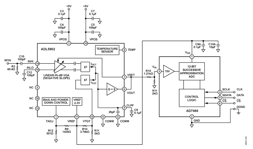
该电路使用 ADL5902 TruPwr™ 检波器测量RF信号的均方根信号强度,信号波峰因素(峰值均值比)在约65 dB的动态范围内变化,工作频率为50 MHz至9 GHz。
测量结果在12位ADC(AD7466)输出端以串行数据形式提供。在数字域中针对环境温度执行简单的4点系统校准。
RF检波器与ADC之间的接口很简单,由两个信号调整电阻组成,无有源元件。此外,ADL5902内部2.3 V基准电压为微功耗ADC提供电源和基准电压。AD7466无流水线延迟,可作为只读SAR ADC。
整个电路实现了约±0.5 dB的温度稳定性。
显示的数据是针对在−40°C至+85°C温度范围内工作的两个器件。

电路描述
测量的RF信号施加于ADL5902的输入端,即dB线性rms响应均方根检波器。外部60.4 Ω电阻R3结合ADL5902的较高输入阻抗,确保宽带50 Ω与RF输入匹配。ADL5902以所谓的“测量模式”配置,VSET和VOUT引脚相连。在此模式下,输出电压与输入均方根值的对数成比例。换言之,读数以分贝值直接呈现,每到十倍调整至1.06 V,或者53 mV/dB。
AD7466 12位ADC的电源电压和基准电压由ADL5902内部2.3 V基准电压源提供。由于AD7466消耗的电流极少(以10 kSPS采样时仅为16 μA),ADL5902的基准电压输出足以向ADC以及由R9、R10、R11、R12组成的温度补偿和均方根精度调整网络供电。
ADC满量程电压等于2.3 V。最大检波器输出电压(在线性输入范围内工作时)约为3.5 V(参见ADL5902数据手册图6、7、8、12、13及14),因此在驱动AD7466前必须降低0.657倍。这个降低过程通过简单的电阻分压器R10和R11(1.21 kΩ和2.0 kΩ)来实现。以上数值可实现0.623的实际比例因子,通过建立电阻容差余量确保ADL5902 RF检波器不会过驱ADC。
图2显示的是检波器输出电压与输入功率的典型曲线(无输出调整)。

该检波器的传递函数可通过以下公式计算近似值:
VOUT = SLOPE_DETECTOR × (PIN − INTERCEPT)
其中SLOPE_DETECTOR是检波器斜率,单位为mV/dB;INTERCEPT 是x轴截距,单位为dBm;PIN是输入功率,单位为dBm。
在ADC输出端,VOUT由ADC输出代码取代,公式可改写为:
CODE = SLOPE × (PIN − INTERCEPT)
其中 SLOPE 是检波器、调整电阻及ADC的组合斜率,单位为次/dB; PIN 和 INTERCEPT 单位仍为dBm。
图3显示的是典型检波器输入功率的功率扫描以及在700 MHz输入信号下观察到的ADC输出代码。

总体斜率和截距随系统的不同而变化,该变化是由RF检波器、调整电阻和ADC传递函数的器件间差异造成的。因此需要系统级校准以确定整个系统的斜率和截距。本应用中,使用4点校准校正RF检波器传递函数内的某些非线性,特别是在低端位置。该4点校准方案产生三个斜率和三个截距校准系数,这些数值在校准后应存储在非易失RAM (NVM)内。
通过向ADL5902施加四个已知信号电平执行校准,从ADC测量相应的输出代码。选择的校准点应在器件线性工作范围内。本例中,校准点位于0 dBm、−20 dBm、−45 dBm及−58 dBm。
斜率和截距校准系数通过以下公式计算:
SLOPE1 = ( CODE _1 – CODE_2)/(PIN_1 − PIN_2)
INTERCEPT1= CODE_1/(SLOPE_ADC × PIN_1)
接着使用CODE_2/CODE_3和CODE_3/CODE_4重复计算,分别得出SLOPE2/INTERCEPT2和SLOPE3/INTERCEPT3。六个校准系数应与CODE_1、CODE_2、CODE_3、CODE_4一起存储在NVM内。
当电路在现场工作时,这些校准系数用于计算未知的输入功率电平PIN,公式如下:
PIN = (CODE/SLOPE) + INTERCEPT
为了在电路工作期间获得适当的斜率和截距校准系数,从ADC观察到的CODE必须与CODE_1、CODE_2、CODE_3、CODE_4进行比较。例如,如果来自ADC的CODE在CODE_1与CODE_2之间,则应使用SLOPE1和INTERCEPT1。该步骤还可用于提供欠量程或超量程警告。例如,如果来自ADC的CODE大于CODE_1或小于CODE_4,表示测得的功率在校准范围以外。
图3还显示了电路传递函数变化与以上直线公式的关系。该误差函数由传递函数边沿弯曲、线性工作范围内的小纹波以及温度漂移造成。误差以dB表示,公式如下:
误差 (dB) = 计算的RF功率 − 实际输入功率
= (CODE/SLOPE) + INTERCEPT – PIN_TRUE
图3还包括了误差与温度的关系曲线。本例中,将在+85°C和−40°C下测得的ADC代码与环境温度下的直线公式进行比较。该方法与现实系统一致,系统校准一般只能在环境温度下进行。
图4和图5分别显示电路在1 GHz和2.2 GHz下的性能。


该电路或任何高速电路的性能都高度依赖于适当的PCB布局,包括但不限于电源旁路、受控阻抗线路(如需要)、元件布局、信号布线以及电源层和接地层。(有关PCB布局的详情,请参见 MT-031教程, MT-101教程 和 高速印刷电路板布局实用指南 一文 。)
常见变化
对于需要较小RF检波范围的应用,可以使用 AD8363 均方根检波器。AD8363检波范围为50 dB,工作频率最高达6 GHz。对于非均方根检波应用,可使用AD8317/AD8318/ AD8319或 ADL5513 。这些器件提供不同的检波范围,输入频率范围最高达10 GHz(有关详情参见 CN-0150)。
AD7466是单通道12位ADC,采用SPI接口。如果终端应用需要多通道ADC,可使用双通道12位AD7887 。在需要多个ADC和DAC通道的多通道应用中,可使用AD7294 。除提供四路12位DAC输出外,这款子系统芯片还含有4个非专用ADC通道、2路高端电流检测输入和3个温度传感器。电流和温度测量结果经过数字化转换后,可通过I2C 兼容接口读取。
电路评估与测试
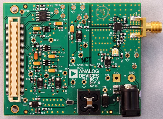
This circuit uses the EVAL-CN0178-SDPZ circuit board and the EVAL-SDP-CB1Z System Demonstration Platform (SDP) evaluation board. The two boards have 120-pin mating connectors, allowing for the quick setup and evaluation of the circuit’s performance. The EVAL-CN0178-SDPZ board contains the circuit to be evaluated, as described in this note, and the SDP evaluation board is used with the CN0178 evaluation software to capture the data from the EVAL-CN0178-SDPZ circuit board.
Equipment Needed
- PC with a USB port and Windows® XP or Windows Vista® (32-bit), or Windows® 7 (32-bit)
- EVAL-CN0178-SDPZ Circuit Evaluation Board
- EVAL-SDP-CB1Z SDP Evaluation Board
- CN0178 Evaluation Software
- Power supply: +6 V, or +6 V “wall wart”
- Environmental chamber
- RF signal source
- Coaxial RF cable with SMA connectors
Load the evaluation software by placing the CN0178 Evaluation Software disc in the CD drive of the PC. Using "My Computer," locate the drive that contains the evaluation software disc and open the Readme file. Follow the instructions contained in the Readme file for installing and using the evaluation software.
Functional Block Diagram
See Figure 1 of this circuit note for the circuit block diagram, and the file “EVAL-CN0178-SDPZ-SCH-Rev0.pdf” for the circuit schematics. This file is contained in the CN0178 Design Support Package.
Setup
Connect the 120-pin connector on the EVAL-CN0178-SDPZ circuit board to the connector marked “CON A” on the EVAL-SDP-CB1Z evaluation (SDP) board. Nylon hardware should be used to firmly secure the two boards, using the holes provided at the ends of the 120-pin connectors. Using an appropriate RF cable, connect the RF signal source to the EVAL-CN0178-SDPZ board via the SMA RF input connector. With power to the supply off, connect a +6 V power supply to the pins marked “+6 V” and “GND” on the board. If available, a +6 V "wall wart" can be connected to the barrel connector on the board and used in place of the +6 V power supply. Connect the USB cable supplied with the SDP board to the USB port on the PC. Note: Do not connect the USB cable to the mini USB connector on the SDP board at this time.
Test
Apply power to the +6 V supply (or “wall wart”) connected to EVAL-CN0178-SDPZ circuit board. Launch the Evaluation software, and connect the USB cable from the PC to the USB mini-connector on the SDP board.
Once USB communications are established, the SDP board can now be used to send, receive, and capture serial data from the EVAL-CN0178-SDPZ board.
The data in this circuit note were generated using a Rohde & Schwarz SMT-03 RF signal source, and an Agilent E3631A power supply. The signal source was set to the frequencies indicated in the graphs, and the input power was stepped and data recorded in 1 dB increments.
Temperature testing was performed using a Test Equity Model 107 environmental chamber. The CN0178-SDPZ evaluation board was placed in the chamber via a slot in the test chamber door, with the SDP evaluation board extending outside.
Information and details regarding how to use the evaluation software for data capture can be found in the CN0178 Evaluation Software ReadMe file.
Information regarding the SDP board can be found in the SDP User Guide.
讨论
- 加入我的myAnalog 登录 myAnalog