LTC4100 4 节锂离子智能电池充电器 (在 4A)
详情介绍


概览
设计资源
设计集成文件
- Schematic
- Bill of materials
- Gerber files
- Allegro layout files
- Assembly drawing
评估硬件
产品型号带"Z"表示符合RoHS标准。评估此电路需要下列选中的电路板
- EVAL-CN0399-SDPZ ($150.00) Battery or USB Powered 9 kHz to 6 GHz RMS Power Measurement System
- EVAL-SDP-CS1Z ($49.00) Eval Control Board
驱动/参考代码
Software such as C code and/or FPGA code, used to communicate with component's digital interface.
AD7091R - No-OS Driver for Renesas Microcontroller Platforms
AD7091R - No-OS Driver for Microchip Microcontroller Platforms
优势和特点
- RMS Power Measurement: 9kHz to 6GHz
- 45dB input power range: −30dBm to +15dBm
- USB powered
电路功能与优势
The circuit shown in Figure 1 is an RF power measurement circuit that accurately measures the power from an RF signal source within a frequency range of 9 kHz to 6 GHz, and has a nominal input power range of 45 dBm (−30 dBm to +15 dBm).
This circuit constitutes a complete rms RF power meter in a tiny form factor that can be powered entirely from a 5 V USB power supply. The measurement signal chain consists of an rms responding RF power detector and a 12-bit, precision analog-to-digital converter (ADC). These devices are powered by a CMOS linear regulator which generates 3.3 V from the 5 V USB supply.
A simple calibration routine can be performed at multiple frequencies to compensate for any frequency response variation of the circuit. Calibration data is stored in a lookup table, which is referenced during the RF power measurement.

电路描述
An RF signal ranging from 9 kHz to 6 GHz is applied to the SMA measurement head of the circuit. This signal drives the RFIN input pin of the ADL5904, an rms responding RF power detector, through an ac coupling capacitor. The size of this capacitor (0.47 μF) sets the minimum input frequency of the circuit. The output voltage from the detector (VRMS) is a dc output voltage level that is proportional to the rms level of the input signal.
The output of the detector directly drives the input of the AD7091R 12-bit ADC. The ADC samples the input periodically and converts the voltage to a digitized voltage code. Each code is transferred to a PC via 3-wire serial peripheral interface (SPI), which uses an equation to calculate the RF power of the input signal. Calibration coefficient information is stored in a look-up table on the PC. The coefficient slope and intercepts are selected based on the frequency of operation, which must be known to accurately calculate the RF input power level.
RF Power Detector
The ADL5904 is a broadband rms responding RF power detector operating from dc to 6 GHz. A functional block diagram of the ADL5904 is shown in Figure 2.
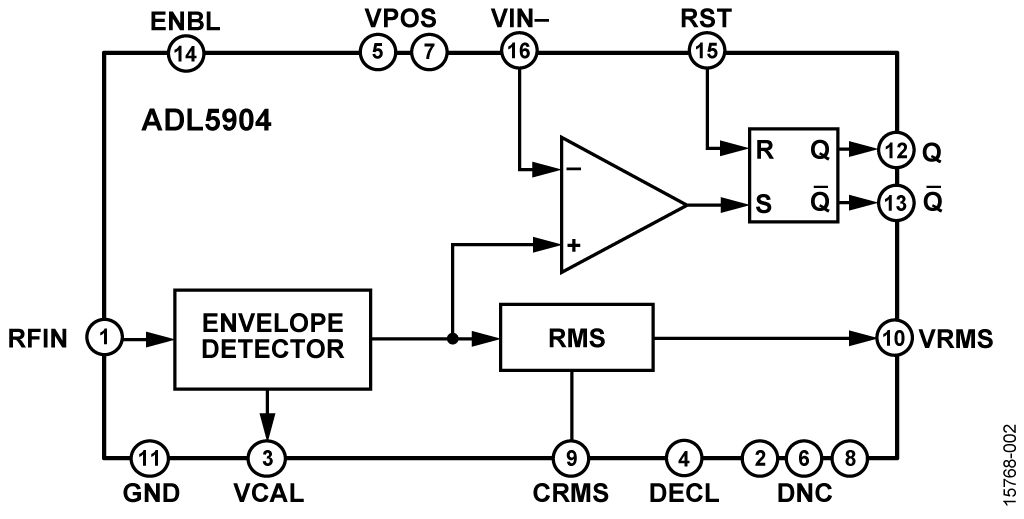
The detector has a dynamic range of 45 dB, ranging from −30 dBm to +15 dBm with a linear-in-dB output characteristic. The low current consumption of 3 mA, makes the ADL5904 a suitable detector for this application circuit where the circuit is powered entirely from the 5 V USB interface from a PC.
An additional function provided by this detector is programmable envelope threshold detection. Threshold detection uses an internal comparator to compare the input envelope voltage with a predefined user input voltage. If the envelope voltage exceeds this predefined voltage, a digital output signal is asserted high. The output signal is latched high through an R/S flip-flop until the reset pin (RST) on the detector is pulsed high. This functionality is not used in the circuit shown in Figure 1.
Analog-to-Digital Converter
The AD7091R shown in Figure 3 is a 12-bit, single-channel successive approximation register (SAR) ADC. It has an ultralow power consumption of 1 mW in normal operation.
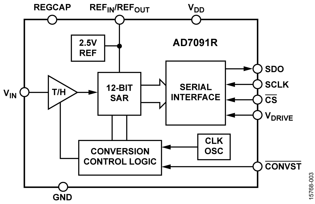
The REFIN/REFOUT pin of the ADC can be overdriven with an external reference voltage. However, in this application, accuracy is not compromised by using the internal 2.5 V reference. Using the 2.5 V internal reference means that the LSB size is

This means that the ADC has a resolution of 610 μV. The input voltage, VIN, to the ADC can range from 0 V to 2.5 V (VREF). Because the maximum output voltage of the detector is approximately 1.8 V, voltage scaling at the input of the ADC is not necessary, allowing the detector output to be connected directly to the ADC input.
On-Board Regulator
The ADP160 is a CMOS linear regulator, which can provide a stable output voltage from 2.2 V to 5.5 V with an ultralow output current quiescent current of 42 μA.

The ADP160 is available in fixed or adjustable configurations. The 3.3 V fixed model used in this design provides a stable output to supply the power detector and ADC, with minimal external circuitry required, as shown in Figure 4.
Power Calculation
The equation used to calculate the power of the RF input signal as a power ratio in decibels (dBm) from the output of the detector is written as follows:

where:
VRMS is the output voltage of the detector as shown in Figure 5.
m is the slope of the power detector.
Int is the x-axis intercept of the power detector.
Using Equation 1, the overall system transfer function becomes

where:
CODERMS is the digitized code representation of VRMS from the ADC, as shown in Figure 5.
m' is the slope of the combined power detector and ADC.
Int' is x-axis intercept of the combined power detector and ADC.

The slope and intercept within the equation are both frequency dependent parameters. As a result, calibration must be performed across frequency, that is, at enough frequency increments to ensure good system flatness across frequency.

Figure 6 shows a plot of the raw measured ADC code versus input power to the detector. Multiple operating frequencies were plotted within the range of the power detector. These measured ADC codes correspond to the sampled and converted output voltage of the power detector. Each plot shown in Figure 6 shows how the characteristic curve of the detector varies linearly with decibel input power, within the operating range of the detector (−30 dBm to +15 dBm). This response is known as a linear-in-dB power detector response.
Software Interface
A simple software graphical user interface (GUI) is used to calculate and display the RF power being measured. Figure 7 shows the front panel of the GUI.

In the Power Measurement tab, the frequency of the input signal must be entered prior to measurement, thereby telling the software which set of calibration coefficients (slope and intercept) to use. The software uses the calibration coefficients that are closest in frequency to the input frequency. Selecting Continuous and clicking Read periodically updates the measured power. A user defined reference level offset can be applied to the measurement to account for external cabling or coupling losses. This offset is added to the measured value, which is then displayed as the power.
Calibration Routine
Before performing a power measurement, the user must perform a calibration routine across frequency.

Figure 8 shows the Calibration tab. A frequency is selected using the numeric selection box. Three power levels are then applied at that frequency. This 3-point calibration routine calculates two different slope and intercept values for the calibration frequency. These values are stored in the look-up table and used for power calculation. Figure 9 shows an example of calibration data for a selected frequency.

Each of the calibration points have a corresponding measured ADC code, as shown in Figure 9. These codes are used to calculate a slope and intercept value for each of the two regions between the calibration power levels. Calibration values stored for each calibrated frequency contain a slope and intercept for these two power regions, as shown in the look-up table outline in Figure 10.

Measurement Sequence
Figure 11 shows the measurement sequence executed during power measurement.

When the user clicks Read, the set of calibration values for the calibration frequency closest to the selected operating frequency are read from the look-up table.
These calibration values contain slope and intercepts for the two power regions of the 3-point calibration routine. The raw ADC code is then read through the SPI interface. This code is used for the power calculation. The slope and intercept from one of the two power regions are extracted from the calibration values for the selected frequency, based on the raw ADC code read.
With these slope and intercept values, power is then calculated using Equation 1 and displayed in the GUI. If the Continuous checkbox is selected, the measurement is repeated periodically for the selected frequency.
Measurement Timing
The timing of each measurement is shown in Figure 12. The ADC is sampled after the convert start (CONSTB) input is asserted low using a GPIO on the SDP-S interface board. After approximately 1 ms, the resultant ADC code value corresponding to the sampled voltage is transferred over the SPI. After calculating power, the GUI display is updated with the current power measurement. The measured power is displayed on the GUI for 1 sec. If measuring continuously, the measurement is repeated.

A complete set of documentation for the EVAL-CN0399-SDPZ board including schematics, layout files, and bill of materials can be downloaded from www.analog.com/CN0399-DesignSupport.
Test Results
After performing the calibration routine at different frequencies, measurement data was manually gathered over the entire power range of the detector to verify that the detector circuit was measuring power accurately.

As shown in the results in Figure 13, the circuit tracks the input power accurately from 10 MHz to 6 GHz. Over this frequency range, the maximum deviation from the actual input power was determined to be 0.57 dB at 5 GHz.
常见变化
At low input power levels (below −20 dBm), the nonlinearity of the transfer function of the ADL5904 increases, suggesting that calibration points can be placed in this region. Note that there is no requirement or benefit in spacing the calibration power levels at even intervals.
If USB power was not available from the port of the PC, as an alternative, a 3.3 V supply can be provided externally to the circuit via the VPOS and GND test points. If an external supply is used, R15 is removed to isolate the on-board regulator output.
Instead of using the internal 2.5 V reference, an external reference source can be supplied to the VREF pin of the ADC to increase the reference voltage or to provide a more stable reference.
An alternative method of reading from the ADC is to use the serial port (SPORT) interface protocol. Using SPORT requires that the larger SDP-B interface board (EVAL-SDP-CB1Z) be used. Custom software must also be programmed for use with the SPORT interface. This option is useful for applications that require faster throughput rate, because using the SDP-B interface board provides up to 1 MSPS throughput.
电路评估与测试
The following equipment is needed to perform the evaluations described in this circuit note:
- EVAL-CN0399-SDPZ evaluation board
- SDP-S board (EVAL-SDP-CS1Z)
- Signal generator (with output frequency within the range of dc to 6 GHz)
- CN-0399 Evaluation Software, which can be downloaded from ftp://ftp.analog.com/pub/cftl/CN0399/
- PC running Windows® 7 connected to the SDP-S board via a USB cable (supplied with the EVAL-SDP-CS1Z)
Setup and Test
To set up and test the EVAL-CN0399-SDPZ board, connect the SDP-S board to the EVAL-CN0399-SDPZ board and connect the USB cable from the PC to the SDP-S board.
- Turn on the signal generator and ensure that the RF output signal is off.
- Directly connect the RF output of the signal generator to the input of the RF power meter board.
- Open the evaluation software, ADL5904 Low Power RF Power Meter.exe, and click Connect.
- Click the Calibration tab in the software window, and begin the calibration routine by setting the signal generator frequency to 1 GHz, and setting the power level to −20 dBm.
- Turn on the RF output of the signal generator, then click Low Cal. Point in the software window. A dialog box appears indicating that the calibration code has been stored for that power level.
- Repeat Step 4 and Step 5 for each of the calibration points at 1 GHz, adjusting the power level of the signal generator each time.
- Click Calibrate to calculate the slope and intercept values for 1 GHz. This operation stores the values in a look-up table in the software folder.
- On the signal generator, adjust the power level to −10 dBm output.
- In the software window, click the Power Measurement tab.
- Select the Continuous checkbox and click Read.
- The RF Power display box reads −10 dBm at 1 GHz.
- Increase the power level in 1 dB steps from −10 dBm to +15 dBm. In the software window, the power level is read up to +15 dBm.
- To halt measurement, click Stop.
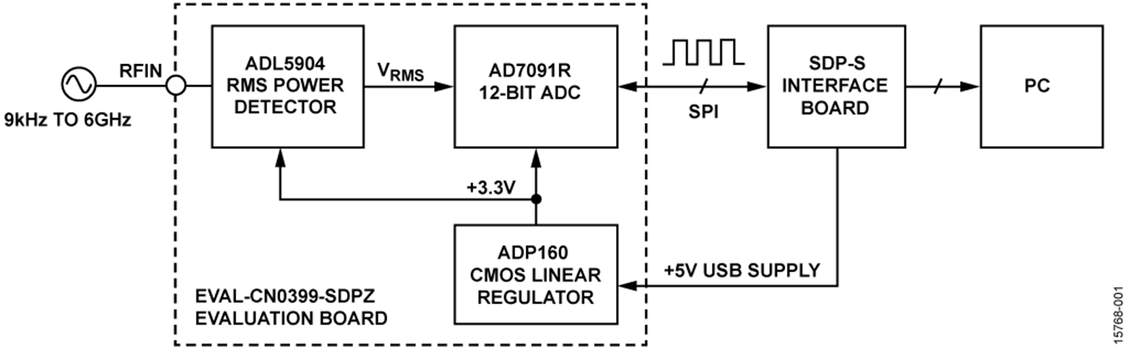
Functional Block Diagram of Test Setup
Figure 14 shows the functional block diagram of the test setup.

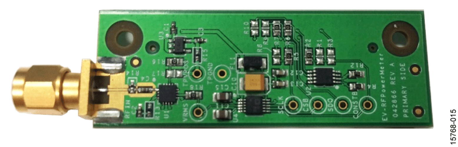
A photograph of the top of the EVAL-CN0399-SDPZ board is shown in Figure 15. The bottom view in Figure 16 shows the EVAL-SDP-CS1Z board connected to the EVAL-CN0399-SDPZ board.


样片申请及购买
样片
| 产品 |
描述 |
可提供样片的 |
| ADP160 | 超低静态电流、150 mA、CMOS线性调节器,提供1.2V至4.2V范围内的15种固定输出电压选项 | ADP160ACBZ-1.2-R7 ADP160ACBZ-1.8-R7 ADP160ACBZ-2.1-R7 ADP160ACBZ-2.5-R7 ADP160ACBZ-2.75-R7 ADP160ACBZ-2.8-R7 ADP160ACBZ-2.85-R7 ADP160ACBZ-3.0-R7 ADP160ACBZ-3.3-R7 ADP160AUJZ-1.2-R7 ADP160AUJZ-1.5-R7 ADP160AUJZ-1.8-R7 ADP160AUJZ-2.3-R7 ADP160AUJZ-2.5-R7 ADP160AUJZ-2.7-R7 ADP160AUJZ-2.8-R7 ADP160AUJZ-3.0-R7 ADP160AUJZ-3.3-R7 ADP160AUJZ-4.2-R7 |
| AD7091R | 1 MSPS、超低功耗、12位ADC、内置片内基准电压源、采用10引脚LFCSP和MSOP封装 | AD7091RBCPZ-RL7 AD7091RBRMZ |
| ADL5904 | 提供包络阈值检测功能的DC至6 GHz、45 dB TruPwr™检波器 |
ADL5904ACPZN-R7 |
- 加入我的myAnalog 登录 myAnalog