LTC3892 具有 10V 栅极驱动的高效率双通道 5V/12V 降压型转换器
详情介绍


概览
设计资源
评估硬件
产品型号带"Z"表示符合RoHS标准。评估此电路需要下列选中的电路板
- EVAL-CN0407-SDPZ ($1249.00) Pico-Ammeter Test System
- EVAL-SDP-CS1Z ($49.00) Eval Control Board
驱动/参考代码
Software such as C code and/or FPGA code, used to communicate with component's digital interface.
优势和特点
- 飞安测量
- 静电计级输入放大器
- 输入偏置电流:20fA(最大值,85°C)
- 24位Σ-Δ型ADC
电路功能与优势
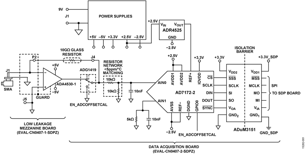
The system functional diagram in Figure 1 is a precision analog front end for measurement of current down to the femtoampere range. This industry-leading solution is ideal for chemical analyzers and laboratory grade instrument where an ultrahigh sensitivity analog front end is required for signal conditioning current output sensors such as photodiodes, photomultiplier tubes, and Faraday cups. Applications that can use this solution include mass spectrometry, chromatography, and coulometry.
The EVAL-CN0407-SDPZ provides a reference design for real-world application by partitioning the system into a low-leakage mezzanine board and a data acquisition board. The input signal conditioning is implemented with the ADA4530-1 on the mezzanine board. The ADA4530-1 is an electrometer-grade amplifier with ultralow input bias current of 20 fA maximum at 85°C. A guard buffer is integrated on the chip to isolate the input pins from leakage to the printed circuit board (PCB). The default amplifier configuration is in the transimpedance mode with a 10 GΩ glass resistor and a metal shield that prevents leakage current from entering any of the high impedance paths on the board. In addition, the mezzanine board includes unpopulated resistor and capacitor pads to allow prototyping with surfacemount feedback resistors as well as other input configurations.
The data acquisition board uses an AD7172-2 24-bit Σ-Δ analog-to-digital-converter (ADC) and is powered from a single 9 V dc supply. The on-board supply generates all necessary voltages required to power both boards. The board connects to a PC via the SDP-S board (EVAL-SDP-CS1Z) and uses digital isolation to prevent noise from the USB bus or ground loops from degrading low current measurements.

电路描述
Low Leakage Mezzanine Board (EVAL-CN0407-1-SDPZ)
The mezzanine board (EVAL-CN0407-1-SDPZ) is built on a hybrid FR-4 and Rogers 4350B laminate for the lowest possible current leakage. The outer two layers are ceramic (Rogers 4350B), and the inner layer is a standard glass epoxy laminate (FR-4). The Rogers 4350B material provides superior insulation resistance in the presence of humidity when compared to glass or epoxy materials. It also minimizes current leakage and has much shorter dielectric relaxation times than glass or epoxy dielectrics. For more information on dielectric relaxation, see the ADA4530-1 data sheet.
Figure 2 shows the board layers stackup. All of the sensitive traces are on the top layer, surrounded by guard traces, vias, and planes.


| Component | Value |
| R1 | 0 Ω |
| R2, R3, R4, R6 | Open |
| R5 | 0 Ω |
| Feedback Resistor | A 10 GΩ glass resistor is placed on the Teflon supports of the main board. One of its leads (the high impedance lead) is plugged into the single pin socket, P2, on the mezzanine board, and the other is soldered to J4 on the data acquisition board (this is a low impedance node). |
With a 10 GΩ feedback resistor and an output voltage range of 4.96 V, the corresponding input current range is ±496 pA.
Transimpedance Amplifier Configuration with SMT Resistor
For applications that may not need the low leakage afforded by a glass resistor, R2 is a combined footprint that allows using an SMT resistor of 0805, 1206, 1210, or 2510 size. The transimpedance amplifier configuration is shown in Figure 4.
In this configuration, remove the glass resistor lead from P2 on the mezzanine board and use the desired resistor at R2 instead. In this configuration, a small metal shield (provided separately) that fits over just the mezzanine board results in a smaller profile, and the mezzanine board can be removed to be evaluated either individually or as part of an end system separate from the data acquisition board.

Buffer Configuration for High Impedance Voltage Output Sensors
The mezzanine board also includes pads to configure the amplifier as a buffer or noninverting amplifier for high impedance voltage output sensors. To configure the board for voltage conditioning, connect a solid wire from the center pin of the SMA connector to the +IN pad and use the settings in Table 2.
| Component | Value |
| R1, R5, R6 | Open |
| R2, R3 | Values for Desired Gain |
| R4 | 0 Ω |
With the settings in Table 2, the SMA shield is connected to the guard voltage. Use the poke-home connector, J5 (bottom side of mezzanine board), to connect a ground reference to the circuit.
When the board is configured in voltage buffer mode, as shown in Figure 5, the output is limited to approximately −4.96 V to +3.5 V because of the common-mode input voltage range of the ADA4530-1. If the amplifier is configured with closed-loop gains larger than 1, the input range must be limited to maintain the common-mode range of the amplifier inputs.

Data Acquisition Board (EVAL-CN0407-2-SDPZ)
The data acquisition board (EVAL-CN0407-2-SDPZ) contains power management, digital isolation, a 24-bit ADC, and a precision voltage reference. In addition to mating with the mezzanine board, this board also mates with the SDP-S board, which in turn connects to a PC via a USB connection. A detailed schematic and layout of the data acquisition board can be found in the CN-0407 Design Support Package at www.analog.com/CN0407-DesignSupport.
Power Management
Figure 6 shows a simplified diagram of the power management section that is located on the data acquisition board. A 9 V dc external power supply, connected to the J1 barrel connector, powers the mezzanine board, ADC, and digital isolation section. The input circuitry includes protection against overvoltage transients and against reverse voltage. Three ADP7118 low noise linear regulators generate 5 V for the ADA4530-1, 2.5 V for the analog front end of the AD7172-2 ADC, and 3.3 V for the digital input/output lines and the isolators. The SDP-S board provides power for the isolated section of the board.

An on-board LED provides an indication that power is on and the system is working correctly. Because some applications may use sensitive light sensors, the evaluation software includes an option to turn off DS1 while the board is acquiring data.
The inverting buck regulator built around the ADP2442 takes the dc input and generates approximately −5.8 V. The switching controller operates in fixed frequency mode (forced PWM), which results in lower efficiency (when compared with pulse-skipping mode) but maintains a constant switching frequency at close to 1 MHz, which makes it easy to filter out. Because the entire system consumes less than 5 mA from the negative supplies, the low power supply efficiency is not a concern.
The output of the inverting buck regulator supplies two ADP7182 negative linear regulators to provide −2.5 V for the AD7172-2 and −5 V for the ADA4530-1.
A detailed schematic and layout of the data acquisition board including the power management circuits, can be found in the CN-0407 Design Support Package at www.analog.com/CN0407-DesignSupport.
ADC and Reference
The output of the mezzanine board has an output voltage range of up to ±5V, whereas the AD7172-2 ADC has an input range of ±2.5 V. A 10 kΩ/10 kΩ matched resistor divider attenuates the output of the mezzanine board by a factor of two. To minimize any offset errors due to the ADC, an ADG1419 single-pole/double-throw (SPDT) analog switch shorts the input of the resistor divider to ground and allows the software to measure the offset error due to the ADC and resistor divider. When offset cancellation is enabled, the software subtracts the measured offset from every reading. Any remaining offset is due only to the ADA4530-1 circuitry.
The GPIO0 digital line (EN_ADCOFFSETCAL) from the AD7172-2 controls the position of the ADG1419 switch. The software writes to register GP_DATA0, resulting in either a 0 or 1 output on GPIO0. The output is referenced to −2.5 V; therefore, the ground pin of the ADG1419 is connected to −2.5 V rather than ground.
The ADR4525 provides a low noise, high accuracy reference to the ADC. The ADC front end is powered from ±2.5 V; therefore, the ADR4525 GND pin is also tied to the −2.5 V supply. This connection develops the 2.5 V reference voltage between the REF+ and REF− pins of the AD7172-2.
Trigger In and Trigger Out
The EVAL-CN0407-SDPZ board includes trigger in and trigger out controls to simplify interfacing the board to external equipment. Both the trigger in and trigger out signals use standard TTL levels.
When trigger in is enabled through software, the system waits for a rising edge on trigger in before starting to acquire data. Similarly, when trigger out is enabled, the system outputs a rising edge when starting to acquire data.
Cleaning and Handling the Mezzanine Board
It is important to always handle the mezzanine boards by the edges and never touch the area within the SHIELD1 shield outline.
If any rework is done to components on the mezzanine board, the board must be properly cleaned to remove any contaminants, such as solder flux, saline moisture, dirt, and dust, to maintain its low leakage performance. Any contaminants can severely degrade its femtoampere performance.
An effective cleaning procedure consists of the following steps:
- Soak the board in an ultrasonic bath with cleanroom-grade isopropyl alcohol for 15 minutes. Ultrasonic cleaning uses ultrasound at a high frequency, creating cavitation in the cleaning solution. This process helps to remove contaminants on the surface of the board and in areas under soldered components that are hard to reach. The next cleaning steps require using fresh isopropyl alcohol.
- Remove the board from the ultrasonic bath with a pair of forceps. Rinse and flush the board with isopropyl alcohol to remove any contaminant residue.
- Flood the board with isopropyl alcohol and gently scrub it with an acid brush. Concentrate on areas between the U1 pins, J1, the guard rings, and the area within the shield outline.
- Rinse and flush the board with isopropyl alcohol.
- Use a final flush for the top and bottom of the board with isopropyl alcohol.
- Use compressed dry air to dry the board. Blow air around the U1 pins, the input traces to J1, and the guard ring area. Be sure to direct the compressed air under J1 and U1 as well.
- To make sure that the board is completely dry, bake the board in the oven at 125°C for 15 minutes.
- After cleaning, remember to place the metal shield on the board. The metal shield helps prevent any contact to the guarded area.
电路评估与测试
This circuit uses the EVAL-CN0407-SDPZ evaluation board and the SDP-S system demonstration platform (EVAL-SDP-CS1Z) evaluation board.
The evaluation software communicates with the SDP-S board to capture data from the EVAL-CN0407-SDPZ.
Equipment Needed
The following equipment is needed:
- PC with USB port and Windows® XP, Windows Vista (32-bit), or Windows 7 (32-bit)
- EVAL-CN0407-SDPZ evaluation board, includes low leakage mezzanine board (EVAL-CN0407-1- SDPZ) and data acquisition board (EVAL-CN0407-2-SDPZ)
- SDP-S board (EVAL-SDP-CS1Z)
- 9 V dc power supply or wall wart
- EVAL-CN0407-SDPZ evaluation software, available for download at ftp://ftp.analog.com/pub/cftl/CN0407/
In addition, a high quality coaxial cable assembly to connect the desired signal to the board is recommended.
Functional Block Diagram of Test Setup
Figure 7 shows a functional block diagram of the test setup.

Getting Started
Download the evaluation software (available at ftp://ftp.analog.com/pub/cftl/CN0407/) and install it by running the setup.exe file.
Connect the EVAL-CN0407-SDPZ and SDP-S boards together, and connect the SDP-S board to the PC with a USB cable. Connect the 9 V dc power supply to the EVAL-CN0407-SDPZ board and load the user interface installer software, named CN0407 Evaluation Software, located under Program Files, Analog Devices. When USB communications are established, the SDP-S board can send, receive, and capture serial data from the EVAL-CN0407-SDPZ.
The SDP-S user guide (UG-291) contains additional information regarding the SDP-S board.
The AN-1373 application note provides more information regarding low current measurements.
Running the Evaluation Software
The evaluation software has a Sampled Data tab where time and frequency domain data are displayed, and a Configuration tab that allows setting parameters such as triggering, offset correction, board configuration, and manual calibration.
Configuration Tab
Figure 8 shows the Configuration tab. The Triggering section includes a graphical depiction of the trigger functionality. Select the desired check boxes to enable the trigger in or trigger out, and enter the desired delay between the trigger in signal, the trigger out signal, and when the ADC starts acquiring data. Select the Offset Cancellation box to measure and remove the offset error due to the ADC input offset and input bias current.

Set the Board Configuration (in the Amplifier Configuration & Calibration Parameters section) to match the configuration of the amplifier on the mezzanine board. Because the amplifier ships configured in transimpedance mode, the default setting is Current Input. In this mode, the feedback resistor control is visible to allow changing it to values different from the factory configuration. By default, it is set to 10 GΩ. The Full Scale Input Range value represents the full-scale input of the system, referred to the input, and it is calculated based on the value of the feedback resistor or the specified gain when configured as a voltage buffer.
In addition to the offset compensation, the user can also apply manual system calibration by providing a gain and offset value. By default, Offset Adjustment is set to 0 and Gain Adjustment is set to 1. The data presented in the evaluation software corresponds to the following equation:
Output Measurement = (Raw Reading + Offset Adjustment) × Gain Adjustment
The LED Configuration section of the Configuration tab controls the LEDs on the board. Clicking General Purpose LED turns the corresponding LED, DS2 (refer to corresponding detailed schematic from the CN-0407 Design Support Package), on and off. Clicking General Purpose LED is a quick way to verify that the system is communicating with the evaluation software. In addition, Turn off Board LEDs During Sampling turns off the power (DS1) and general-purpose LED (DS2) while the ADC is acquiring data. When using a photodiode or other light sensors, turning off the LEDs on the board may improve the measurements.
Sampled Data Tab

The Sample Rate dropdown box selects the ADC output data rate between 0.83 SPS and 867.3 SPS.
After selecting the desired sampling rate, select the acquisition buffer size in seconds. This selection determines how much data is displayed on screen and retained in memory. Click Start Sampling to begin acquiring data from the board. For output data rates of 19.99 SPS and slower, the display is updated continuously as a rolling window. For output data rates greater than 19.99 SPS, the update rate of the chart is equal to the time duration of the acquisition window. The status bar at the bottom of the screen counts down the time remaining until the next update.
In Continuous acquisitions, the system continues to acquire data until the user clicks Stop Sampling. In Single acquisition, the system stops after reaching the specified Buffer Size.
Above the Start Sampling button, indicators display time domain information such as the dc value of the signal and the standard deviation. When measuring a dc input, the standard deviation is equal to the rms noise of the signal.
The lower section of the Sampled Data tab displays the frequency domain data from the system. The controls on the right configure the frequency domain chart as either power spectrum or power spectral density. The user can also configure the type of window, enable averaging, and configure the number of averages to perform. When displaying the power spectrum plot, use the Y-axis scaling control to set the Y-axis units to either dB of full scale or linear units (volts or amps, depending on the board configuration).
Click Save Data To CSV File to save the current time and frequency domain charts to two comma separated files.
Testing the System
Connect the external power supply and launch the evaluation software. The software is able to communicate with the EVAL-CN0407-SDPZ if the Analog Devices system development platform driver appears in Windows Device Manager. When USB communications are established, the SDP-S board can send, receive, and capture serial data from the EVAL-CN0407-SDPZ.
To measure system noise, make sure the shield is installed on the board, and do not connect anything to the input SMA connector. For best performance, place the entire assembly inside a metal box, which is electrically connected to ground.
In the Configuration tab, check the Offset Cancellation box, and make sure that the system is configured as Current Input with a 10 GΩ resistor. In the Sampled Data tab, select the desired sampling rate from the dropdown box and click Start Sampling. Thermal noise from the 10 GΩ resistor can dominate system noise; therefore, for best performance, select the lowest acceptable sampling rate. For example, Figure 10 shows the system noise when sampling at 0.83 SPS for 120 minutes. The resulting rms noise is 1.4 fA with a dc value of −150 aA.

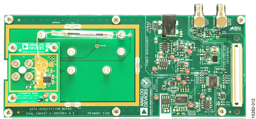
Figure 11 and Figure 12 show photographs of the EVALCN0407-SDPZ, including the low leakage mezzanine board and the data acquisition board.


样片申请及购买
样片
| 产品 |
描述 |
可提供样片的 |
| ADUM3151 | 用于SPI的3.75 kV、7通道、SPIsolator数字隔离器(2/1辅助通道方向性) | ADUM3151ARSZ ADUM3151BRSZ |
| ADP7182 | -28V、200MA、低噪声、线性稳压器 | ADP7182ACPZ-5.0-R7 ADP7182ACPZ-R7 ADP7182ACPZN-1.2R7 ADP7182ACPZN-1.5R7 ADP7182ACPZN-2.5R7 ADP7182ACPZN-5.0R7 ADP7182ACPZN-R7 ADP7182AUJZ-1.8-R7 ADP7182AUJZ-2.5-R7 ADP7182AUJZ-3.0-R7 ADP7182AUJZ-5.0-R7 ADP7182AUJZ-R7 |
| ADR4525 | 超低噪声、高精度2.5V基准电压源 | ADR4525ARZ ADR4525BRZ ADR4525WBRZ-R7 |
| AD7172-2 | 集成真轨到轨缓冲器的低功耗、24位、31.25 KSPS、Σ-Δ型ADC | AD7172-2BRUZ |
| ADA4530-1 | 微微安输入偏置电流静电计放大器 | ADA4530-1ARZ |
- 加入我的myAnalog 登录 myAnalog