LT6375 27dB 音频增益级
详情介绍

概览
产品详情
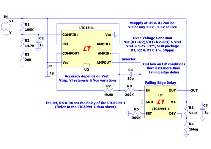
一款抑制毛刺干扰的过压检测器是采用 LTC1541 微功率运放 + 比较器 + 电压基准和 LTC6994-1 TimerBlox® 延迟模块 / 防反跳器构建而成。在该电路中,LTC1541 比较器负责检测电源轨过压情况 (包括毛刺干扰)。内置运放对该信号进行反相并驱动对低电平有效过压信号实施防反跳处理的 LTC6994-1,以抑制比某给定延迟周期短的毛刺干扰。延迟周期由 SET 引脚上的单个电阻器设定。LTC1541 和 LTC6994-1 的电源可以是 Vin 或 2.5V 至 5.5V 电压源。该电路的准确度取决于 LTC1541 的 Vref、Vtrip、Vhysteresis 和 Vos 电压的变化。


LTC6994 是一款可编程延迟模块,具有一个 1μs 至 33.6s 的延迟范围。LTC6994 隶属于 TimerBlox 通用型硅定时器件系列。单个电阻器 RSET 编程一个内部主振荡器频率,从而设置 LTC6994 的时基。输入至输出延迟由该主振荡器和一个内部时钟分频器 NDIV 来决定 (可编程至 1 ~ 221 范围内的 8 个设定值)。在延迟了上升和 / 或下降变换之后,输出将跟随输入。LTC6994-1 将延迟上升沿或下降沿。有关 LTC6994 的简易配置,请下载 TimerBlox Designer 工具。LTC6994 采用 6 引脚 ThinSOT 和 DFN 封装。
LTC1541 / LTC1542 将一个微功率放大器、比较器和带隙基准整合在一个 8 引脚封装中。该器件依靠 2.5V 至 12.6V 单电源或 ±1.25V 至 ±6.3V 双电源供电运作,并具有一个 5µA 的典型电源电流。运放和比较器均具有一个从负电源扩展至正电源之 1.3V 以内的共模输入电压范围。运放输出级具有轨至轨输出摆幅。比较器的负输入在内部连接至基准输出。LTC1541 采用 DFN、MSOP 和 SO 封装。
工具及仿真模型
LTspice
LTspice® is a powerful, fast and free simulation software, schematic capture and waveform viewer with enhancements and models for improving the simulation of analog circuits.
To launch ready-to-run LTspice demonstration circuits for this part:
Step 1: Download and install LTspice on your computer.
Step 2: Click on the link in the section below to download a demonstration circuit.
Step 3: If LTspice does not automatically open after clicking the link below, you can instead run the simulation by right clicking on the link and selecting “Save Target As.” After saving the file to your computer, start LTspice and open the demonstration circuit by selecting ‘Open’ from the ‘File’ menu.
